Choosing a detector requires evaluating many operating parameters and desired outcomes. This introduction provides a series of guideposts that will help lead the way to the right one.
Earl Hergert, Hamamatsu Corporation
Any number of medical, industrial, and analytical applications requires the detection of light. Chemiluminescence, bioluminescence, fluorescence, and atomic absorption are just a few, and all require a detector to convert the light into an electrical signal. There are four basic technologies that accomplish this task: photomultiplier tubes (PMTs), silicon photomultipliers (SiPMs), avalanche photodiodes (APDs), and silicon photodiodes.
The question of which detector to use is not a simple one. In applications where there is ample light, a photodiode is suitable. A PMT is the best choice where there are very weak signals. In other applications, however, the choice is not so clear. This article will examine detector characteristics, criteria for selection of a detector, and amplifier performance, and hopefully, help you to choose.
Detector options
The PMT (Figure 1) consists of a photosensitive surface (photocathode), electron multipliers (dynodes), and a collection electrode (anode) within an evacuated glass or metal envelope. Light enters the input window and is absorbed by the photocathode. An electron is emitted from the cathode and accelerated to the first dynode by an applied voltage. The electron is accelerated to sufficient potential that, when it collides with a dynode, secondary electrons are produced. These secondary electrons are in turn accelerated to the next dynode, with the process being repeated until the electron cloud is collected at the anode.
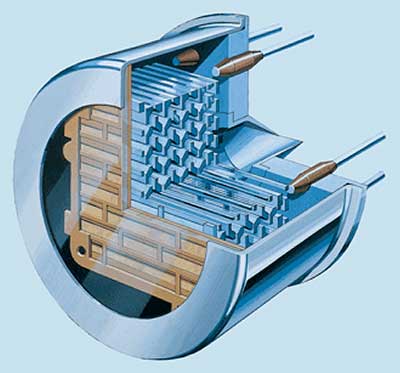
Figure 1. PMTs make good use of metal channel dynodes.
A PMT's gain can be estimated by the following expression:

µ = current amplification (gain)
δ = secondary emission ratio for dynodes
n = number of dynode stages
For a nine-stage PMT with a secondary emission ratio of eight, the current amplification would be about 107. Large gain and low noise make the PMT an attractive detector for many applications. However, it is not the only device to possess internal gain.
A silicon photodiode is essentially a PN junction consisting of a positively doped P region and a negatively doped N region. Between these exists an area of neutral charge known as the depletion region. When light enters the device, electrons in the crystalline structure become excited. If the energy of the light is greater than the bandgap energy of the material, electrons will move into the conduction band, creating holes in the valence band where the electrons were. These electron-hole pairs are created throughout the device. Those generated in the depletion region drift to their respective electrodes: N for electrons and P for holes. This results in a positive charge buildup in the P layer and a negative one in the N layer. The amount of charge is directly proportional to the amount of light falling on the detector. If an external circuit is connected to the P and N electrodes, current will flow. This is the photovoltaic method.
In the photoconductive mode, a reverse bias is applied to the photodetector. This has the effect of increasing the electric field strength between the electrodes and the depth of the depletion region. The advantages are higher speed, lower capacitance, and better linearity; however, the dark current becomes larger. Generally, PIN photodiodes and APDs are operated in this fashion.
The APD (Figure 2) is a specialized silicon PIN photodiode designed to operate with high reverse bias voltages. Large reverse voltages generate high electric fields at the PN junction. Some of the electron-hole pairs passing through or generated in this field gain sufficient energy (greater than the bandgap energy) to create additional electron-hole pairs. This process is known as impact ionization. If the newly created electron-hole pairs acquire enough energy, they also create electron-hole pairs. This is known as avalanche multiplication and is the mechanism by which APDs produce internal gain. Internal gain is an important attribute when the detector is combined with an amplifier.
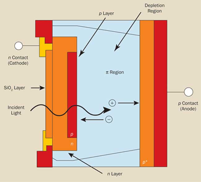
Figure 2. Cross section of an avalanche photodiode.
The silicon photomultiplier (SiPM) has an array of pixels, or microcells, consisting of Geiger-mode APDs connected in parallel (Figure 3). The APD in each pixel of the SiPM is operated above its breakdown voltage to increase the internal gain. At this overvoltage, the APD is stable until an electron enters the avalanche region, resulting in the avalanche region breaking down and the APD becoming a conductor. This is known as a Geiger discharge. The current flow produced by the breakdown is large; therefore, the signal gain (>105) is large because a single electron resulted in a large flow of current.
However, a device that triggers once is not a very useful detector, so a means to stop the breakdown or to reset the APD is required. Typically this is accomplished by placing a “quenching” resistor in series with the APD. When the junction breaks down, large current flows through this resistor, resulting in a voltage drop across the resistor and in the APD. If the voltage drop is sufficient, the APD voltage will drop below the breakdown voltage and be reset. The discharge-and-reset cycle is known as the Geiger mode of operation.
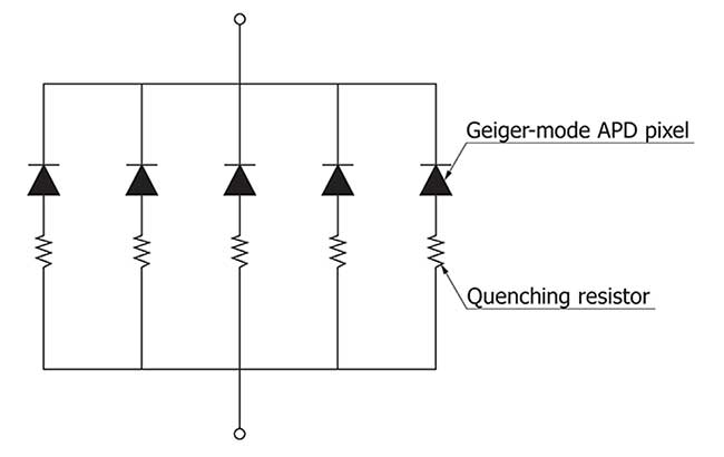
Figure 3. Simplified structure of a silicon photomultiplier (SiPM).
Each pixel in a SiPM outputs a pulse when it detects photons, so the sum of the output from each pixel forms the SiPM’s output. This allows counting single photons or detecting pulses of multiple photons. When photon flux is low and photons arrive at a time interval that is longer than the recovery time of a pixel, the SiPM will output pulses that equate to a single photoelectron. When the photon flux is high or the photons arrive in short pulses (pulse width less than the recovery time), the pixel outputs will add up and equate to 2-photoelectron or 3-photoelectron pulses, for example.
The silicon photomultiplier is a relatively new photodetector technology, and only a few companies manufacture these detectors, including Hamamatsu Photonics. Hamamatsu’s brand of SiPMs is called “Multi-Pixel Photon Counters” (MPPC).
Selection criteria
One of the first, and often overlooked, aspects of choosing a detector is defining the parameters of the application. One should determine the wavelength at which the detector will be used, as well as the light power that will be incident on the device. Frequently, these criteria will limit the options.
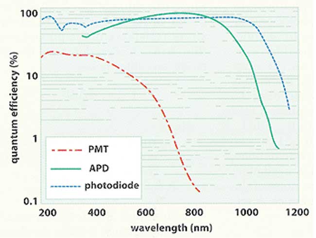
Figure 4. Spectral response of a PMT, APD, and photodiode.
Quantum efficiency (Figure 4) is the intrinsic ability of a detector to convert photons into electrons or holes. It is expressed as the ratio of generated electrons to incident photons in percent. Manufacturers often do not list the quantum efficiency (QE) among their specifications. Instead, they use the radiant sensitivity, given in electrical current generated per incident watt of optical power, amperes per watt (A/W). The QE and photosensitivity have the following relationship:

where
S = radiant sensitivity in A/W
λ = wavelength in nanometers
For SiPMs, manufacturers list photon detection efficiency (PDE) instead of QE. PDE is the product of QE, fill factor, and avalanche probability. Fill factor is the ratio of the photosensitive area to the total area of a SiPM. The avalanche probability is the probability that the charge carriers generated in a pixel may cause avalanche multiplication. PDE is a function of wavelength and reverse voltage (Figure 5).
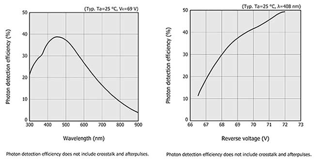
Figure 5. Example plots of a SiPM’s photon detection efficiency (PDE) as a function of wavelength (left) and reverse voltage (right).
In the case where all other detector characteristics are equal, the detector with the highest QE possible is the best choice.
One of the most misunderstood aspects of detectors is gain. Many users mistake large signal amplitude for signal quality. Internal gain in a detector only amplifies the photogenerated signal. If the photogenerated signal is noisy, the amplified signal will be noisy as well. While this seems obvious, it is a common mistake. In reality, the benefit of gain is in raising the photogenerated signal above the noise level of the signal processing equipment. In the case where the signal processing equipment is limiting the signal-to-noise ratio, internal amplification in the detector improves it.
Bandwidth refers to the electrical bandwidth of the detector/signal processing equipment. Most of the noise sources involved with designing an optical detector system are random in nature with very wide frequency distributions. Therefore, all else remaining equal, if the electrical bandwidth is increased, the detector's system noise will increase such that:

The noise problem
When designing a detector system, it is critical to keep the electrical bandwidth as close to the required bandwidth as possible. That is, if the light signal is changing at a frequency of 10 kHz, having a detector system with a bandwidth of 1 MHz will only needlessly introduce noise.
In any light detection application, the lower limit of signal detection is determined by the noise characteristics of the detector and its amplifiers. There are three primary sources of noise in any optical detector system: photon-related shot noise, detector dark noise, and amplifier noise. The first two are related to the detector.
Shot noise is inherent in any signal generated by the detector. Its cause is related to the quantum nature of light. It is expressed by the following equation:

where
inoise = rms noise current
q = electron charge
Iph = photogenerated signal current
M = detector internal gain
F = detector excess noise factor
ΔB = electrical bandwidth of detector amplifier combination
Also contributing to the noise of the system is the detector dark noise, which is unrelated to the signal level. For the PMT and the APD, there are two primary sources of noise in addition to the shot noise created by the signal: shot noise of the dark current generated by the detector and noise created by the gain mechanism (excess noise) of the detector.
The shot noise of the dark current has the same form as equation 4 except that ID is substituted for Iph.
The details of excess noise are beyond the scope of this article. Simply put, it is the noise added to the signal by the internal amplification mechanism of a detector. For the PMT, it has a value of about 1.4 and decreases with increasing gain. For the APD, it has a value greater than 2 and increases with rising gain. It also has a dependence on the wavelength of light being detected.
As noted, there are two methods of operation for a photodiode: the photoconductive and photovoltaic modes. The dominant noise source is different in each case. In the photoconductive mode, the dark current is rather large, so the shot noise of the dark current dominates the noise of the photodiode. To apply the shot noise equation to a photodiode, substitute Idark for Iph and set M and F equal to 1.
In the photovoltaic mode of operation the dark current is negligible. In this case the Johnson noise of the photodiode shunt resistance dominates the noise term.

where
k = Boltzmann's constant
T = absolute temperature of the photodiode
Rsh = shunt resistance of the photodiode
For SiPMs, there are two additional noise sources—afterpulses and crosstalk—that users need to be aware of (Figure 6). An afterpulse occurs when a trapped charge is released in a pixel that is recovering from a primary avalanche, and the released charge triggers a secondary avalanche within that pixel. Afterpulses are delayed in time relative to the primary signal. Optical crosstalk occurs when the primary avalanche in a pixel causes an emission of photons that trigger one or more avalanches in neighboring pixels. Crosstalk pulses are caused by the emission of light and therefore occur “instantly,” and as a result, the crosstalk pulses are superimposed on the signal pulses.
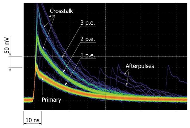
Figure 6. Crosstalk and afterpulses in SiPMs.
Afterpulsing and crosstalk are, in effect, noise, but it is not clear what impact they have on measurement systems because of the nature of these noise sources. One way to minimize their effect is to choose SiPMs with low afterpulsing and crosstalk characteristics.
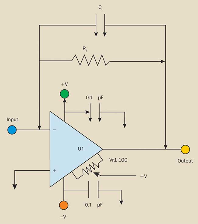
Figure 7. A transimpedance amplifier converts detector output current into a voltage.
The photodetector amplifier (Figure 7) is a major system component and its noise will, in many instances, dominate system noise. To understand the total noise of the detector system, one must understand the noise of the detector amplifier combination. While the derivation of the noise equations for an amplifier are quite complex (see references), some basic assumptions and simplifications can lead to noise equations that are very useful.
The first term is the Johnson noise of the amplifier feedback resistor. Since the value of the feedback resistor must be smaller than the shunt resistance of the photodiode, this term can often dominate the detector amplifier noise.

where
If = rms current due to Johnson noise of amplifier feedback resistance
Rf = feedback resistor
To minimize the Johnson noise, one must choose a large feedback resistor or cool the amplifier.
The second term arises from the input noise voltage of the amplifier, and it takes the following form:

where
Iv = rms current noise due to voltage noise of amplifier
Va = input voltage noise density, for example nV/Hz1/2
Ct = terminal capacitance of the detector
The voltage noise current is interesting in that it is dependent on the terminal capacitance of the detector. It is also strongly related to the frequency bandwidth. To reduce this component or amplifier noise, a detector with low capacitance should be selected. Furthermore, the electrical bandwidth should be minimized.
Finally, the third noise component is the shot noise arising from the amplifier input bias current (Ib). If care is taken in choosing a low input bias current field-effect transistor amplifier, this source of noise is minimized.
The total detector amplifier rms noise becomes:

where
Ishot = detector dark noise + signal-induced shot noise
The amplifier noise plus the detector dark noise represent the noise floor of the detector system, while the signal-induced shot noise varies with signal level. With this in mind, the signal-to-noise ratio can be written as follows:

From the above equation, it can be surmised that the advantage derived from internal gain detectors is in the reduction of the effective noise of the amplifier by the gain of the detector. Therefore, very high gain detectors such as PMTs reduce the amplifier noise contribution to insignificance. Likewise, moderate gain detectors such as APDs greatly reduce the noise contribution of the amplifier to the total noise of the detector system, whereas photodiodes having no internal gain are much more susceptible to the noise of the amplifier.
Modules to the rescue
Today's marketplace demands that products go from the drawing board to the marketplace as fast as possible and at the lowest possible cost. Modules make such goals attainable by maximizing integration, reducing development costs, and saving time.
Modules can be as simple as a photodiode amplifier combination or as complex as a microprocessor-controlled photon-counting unit that includes a PMT, high-voltage power supply, photon-counting electronics, and a computer interface, all in a 6-inch-long package.
An example of a module's advantage is demonstrated in Figure 8. The MPPC is a difficult device to design with for a number of reasons. It is extremely temperature sensitive, its noise increases with increased gain, and it is very sensitive to small changes in bias voltage. The module shown incorporates a very low ripple power supply, low-noise amplifier, temperature feedback circuit (to compensate for thermal drift), and it runs from a 5 V DC supply. The instrument designer has done away with the need to work with high voltage and the need to thermally compensate that high voltage for detector gain drift. As a result, the concentration can be on integrating the detector into an optical system.

Figure 8. Block diagram of a SiPM (MPPC) module.
Still, the module does not help in the selection of a detector but only in making the detector easier to use. Therefore, every designer of electro-optical instruments should be familiar with the detector's performance and use.
Guidelines for detector selection
The following is a simple guide to selecting a detector:
1. Determine the requirements of the application. Some parameters to consider are:
• Light power level
• Wavelength range of incident light
• Electrical bandwidth of the detector amplifier
• Mechanical requirements of the application, such as: size of the instrument (Is a small detector needed?); power consumption of the instrument (Is low power consumption a requirement?); and the operating temperature range of the instrument (Is cooling required?)
• Price
2. Once the detector field is narrowed based on the application, calculate the signal-to-noise ratio under the conditions of the application. Plots like signal-to-noise ratio vs. light power (Figure 9) are convenient for comparing detectors.
3. Confirm calculated results by measuring the signal-to-noise ratio in the application itself. While this procedure seems obvious, in practice it is often omitted. This results in inappropriate detector selection.
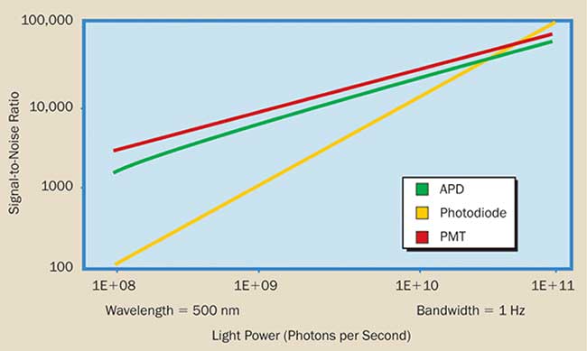
Figure 9. Signal-to-noise ratio vs. light power for a PMT, APD, and photodiode.
In general, the PMT performs best in extremely low light-level conditions in UV to near-IR wavelength ranges. It is ideally suited for fluorescence spectroscopy, such as in immunoassay, chemiluminescence for detection of NOx, and gamma cameras for medical imaging.
The SiPM is essentially between a PMT and an APD, and it performs best in applications involving low light levels in the UV to visible wavelength ranges. Examples include fluorescence measurement in applications such as flow cytometry and DNA sequencing, as well as scintillation measurement in high energy physics experiments and positron emission tomography (PET).
The APD performs best in applications involving low light levels and high-bandwidth applications conducted in the near-IR. Examples include industrial barcode scanning, laser rangefinding, and particle counters.
The photodiode is better suited for applications with low- to moderate-light levels in the UV to near-IR range. Such applications include optical power meters, optical smoke detectors, and optical absorption measurements such as high-performance liquid chromatography.
The ultimate test of a detector system is its signal-to-noise performance in a particular application. It is not the only test to which the detector should be subjected. For instance, in a particular IR application, the APD may have the best S/N ratio but its large temperature coefficients may make it difficult to use. Therefore, the designer might prefer the greater stability of the photodiode despite its low signal-to-noise ratio.
What is more important than deciding which type of detector to use is selecting the right one for that particular application. To this end, the designer must approach the choice of detectors without bias and select what is best.
References
• R.W. Engstrom (1980). Photomultiplier Handbook. RCA Electro-Optics and Devices.
• Hamamatsu Photonics K.K. (1994). Photomultiplier Technical Handbook. Hamamatsu Photonics K.K.
• Hamamatsu Photonics K.K. (1992). How to Perform Photon Counting. Hamamatsu Photonics KK.
• T.E. Jenkins (1987). Optical Sensing Techniques and Signal Processing. Prentice-Hall International.
• J. Gowar (1984). Optical Communication Systems. Prentice-Hall International.
• P.P. Webb, R.J. McIntyre, J. Conradi (1974). Properties of Avalanche Photodiodes. RCA Review.
• R.J. McIntyre (1966). "Multiplication Noise in Uniform Avalanche Diodes." IEEE Transactions on Electron Devices, Vol. 13, pp. 164-168.
• G.F. Knoll (1979). Radiation Detection and Measurement. John Wiley and Sons.
• N. Akil et al. "A Multimechanism Model for Photon Generation by Silicon Junctions in Avalanche Breakdown." IEEE Trans. on Electron Devices, vol. 46, No. 5, pp. 1022 – 1028, May 1999.
• P. Eckert et al. "Characterization studies of silicon photomultipliers", Nucl. Instrum. and Meth. A 620 (2010) 217-26.
• L. Lacaita et al. “On the Bremsstranhlung origin of hot carrier induced photons in silicon devices.” IEEE Trans. Nucl. Dev., vol. 40, No. 3, pp. 577- 582, March 1993.
• R. Newman “Visible light from a silicon p–n junction,” Phys. Rev., vol. 100, no. 2, pp. 700–703, 1995.
• Vacheret et al., “Characterization and simulation of the response of Multi-Pixel Photon Counters to low light levels.” Nucl. Instrum. and Meth. A 656 (2011) 69-83.
• R.H. Haitz “Model for the Electrical Behavior of a Microplasma.” J. of Appl. Phys., vol. 35, no. 2 (1964), pp. 1370-1376.
• R.J. McIntyre “Theory of Microplasma Instability in Silicon.” J. of Appl. Phys., vol. 32, no. 6 (1961), pp. 983-995.
• T. Murase et al. “Development of PPD: characterization and simulation,” International Workshop on New Photon Detectors PD09, June 24-26 2009, Shinshu University, Matsumoto, Japan.
• Y. Musienko et al. “The gain, photon detection efficiency and excess noise factor of multi-pixel Geiger-mode avalanche photodiodes.” 2006 Nucl. Instrum. Meth. A 567 57.
• T. Nagano et al. “Timing Resolution Improvement of MPPC for TOF-PET Imaging.” 2012 IEEE Nuclear Science Symposium and Medical Imaging Conference Record (NSS/MIC).
• K. Yamamoto et al., “Development of Multi-Pixel Photon Counter (MPPC),” IEEE Nuclear Science Symposium, 2007.
/Buyers_Guide/Hamamatsu_Corporation/c5841