Full company details
G&H
 Dowlish Ford
Ilminster
Somerset TA19 0PF
United Kingdom
COMBS Launches with $22.9M Award: Week in Brief: 11/1/24
Photonics.com
Oct 2024MILPITAS, Calif., Nov. 1, 2024 —
Opterro, Inc. has signed a memorandum of understanding with
Gooch & Housego PLC (
G&H), manufacturer of photonic components and systems, aiming to combine Opterro’s fiber-optic distributed systems with G&H’s high-volume manufacturing capabilities to address the needs of industry and government customers across various sectors. The partnership will initially investigate commercial feasibility, with the intent to develop a long-term supply agreement that facilitates the expanding global distribution of Opterro’s sensing systems and end-to-end solutions. President of G&H Stratos Kehayas will also join Opterro’s board of directors as an observer.

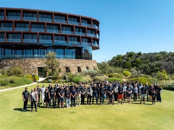
The COMBS research team. Courtesy of RMIT University.
MELBOURNE, Australia — The
ARC Centre of Excellence in Optical Microcombs for Breakthrough Science (
COMBS) has received an AUD $35 million ($22.9 million) award from the
Australian Research Council along with an investment of more than AUD $9 million from
RMIT University where the center will be based. COMBS, which was launched in October, brings together experts from RMIT and eight other universities across Australia in optical physics, optical microcombs, and semiconductor technology in fields such as information processing, navigation, defense, biomedical imaging, environmental sciences, and space exploration.
BOSTON — The Massachusetts state government has awarded ~$5 million to establish a quantum computing complex at the
Massachusetts Green High Performance Computing Center (
MGHPCC) in Holyoke, Mass. The MGHPCC will work with their industry partner,
QuEra Computing Inc., on a two-year project to install and deploy a neutral atom quantum computer. The complex will facilitate open access research and application development across the state, allow for quantum hardware innovation, and provide hands on training and internship opportunities for students.
BOSTON —
Altium SA, a software developer for printed circuit board design, has loaned medical technology company
Phase Holographic Imaging (
PHI) SEK 7 million ($660,000) to repay a previous loan raised from
Bizcap AB earlier this year. The board of directors of PHI and Altium SA, as the main shareholder, are also in discussions regarding alternatives for long-term financing of PHI. These discussions include the convertible loan which was acquired by Altium SA from Fenja Capital (previously Formue Nord) in October 2023.

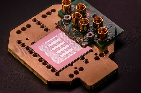
Photonic’s silicon quantum processor. Courtesy of TELUS.
VANCOUVER, British Columbia — Communications technology company
TELUS has entered into a collaboration with quantum company
Photonic Inc. to accelerate the development of next-generation quantum communications in Canada. TELUS will provide Photonic dedicated access to a 30 km fiber-optic network, enabling the testing of quantum technologies.
GHENT, Belgium —
Ardena, a specialist pharmaceutical contract development and manufacturing organization, has established a new bioanalytical lab in Oss, Netherlands, with additional capacity and new GLP capabilities to its Bioanalytical Center of Excellence in Assen, Netherlands. Expected to be operational by early 2025, the 3000+ sq ft lab will provide advanced analytical testing services. Ardena’s investments in Assen will focus on expanding its capabilities in immunochemistry, flow cytometry, and quantitative polymerase chain reaction platforms.

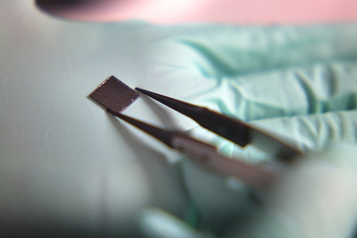
A sample of monolayer III-nitrides on a foreign substrate. Courtesy of the University of Michigan.
ANN ARBOR, Mich. — A research group from the
University of Michigan has been awarded $3 million as part of
DARPA’s Material Synthesis Technologies for Universal and Diverse Integration Opportunities initiative. The group’s project titled, “CMOS compatible, defect-free universal growth of III-N and III-V multilayer heterostructures on Si (001),” will use a new method to grow ultra-thin layers of III-V compound crystals without a foreign metal catalyst, allowing for the growth of semiconductor materials on silicon lattice without defects. The final goal of the project will be to partner with the manufacturing company Intelligent Epitaxy Technology, Inc. to show viability of the material at scale for use in industry.
ORLANDO, Fla. — A research group from
University of Central Florida is leading a project to develop a compact semiconductor light source for defense and civilian applications such as room disinfection. The work is funded through a $1 million grant from the
U.S. Army Combat Capabilities Development Command Army Research Laboratory. The group plans to develop a UVC laser that can last for at least 10,000 h by overcoming the electromigration of defects, which can cut the life of a laser short, and that incorporates scalable superlattice structures.
PLANO, Texas —
Denka Company Limited has made an investment into enethiol optical films developer
Ares Materials through a corporate venture capital fund jointly managed with Pegasus Tech Ventures. Through the investment, the companies will form a partnership in joint development to improve display performance by utilizing Denka’s HARDLOC OP series of enethiol adhesives in combination with Ares’ optical films, with the aim of social implementation in the flexible display field.

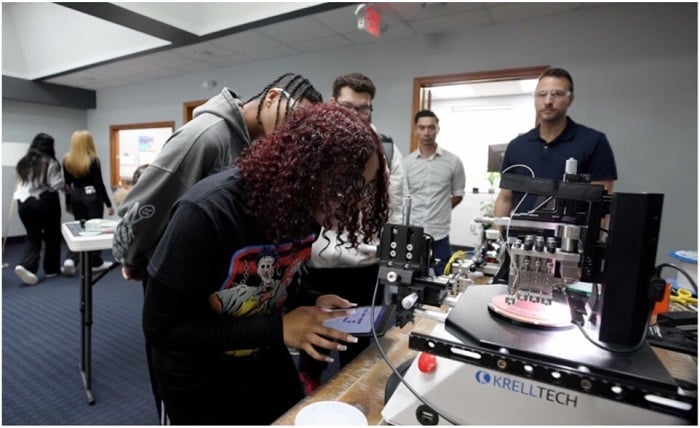
High school students from Pleasantville, N.J. taking part in Krell’s Photonics Outreach Program. Courtesy of Krell Technologies.
NEPTUNE CITY, N.J. — Photonics solutions developer
Krell Technologies has launched its Photonics Outreach Program aimed at high school students. The program was created with the goal of introducing younger generations to the field of photonics in a dynamic and engaging way.