Full company details
Andor Technology
An Oxford Instruments Co.
 Springvale Business Park
7 Millennium Way
Belfast BT12 7AL
United Kingdom
Sensors Capture Image Data from Near and Far
Photonics.com
Dec 2021Factors such as sensitivity, field of view, and speed help to determine which type of imaging sensor, CCD or CMOS, is best suited for a specific application.Alan Mullan and Aleks Marsh, Andor Technology
Imaging sensors reveal key details during the exploration of many areas of science, from untangling events at the quantum level and the fundamental processes of the cell to building our understanding of the wider cosmos. Imaging sensor technologies used in these applications can be grouped into two main types: charge-coupled devices, or CCDs — including electron multiplying CCDs — and complementary metal oxide semiconductors, or CMOSs.

The amount of space debris continues to increase, posing an ever-increasing hazard to important satellites. Image sensors enable debris to be tracked. Courtesy of Andor Technology.
Choosing the right sensor technology for an application can be a daunting task amid the vast array of options to consider, and the choice can affect the performance of the technology in a specific setting. Such options include sensitivity, speed, and field of view, and attention must be paid to sensor parameters such as pixel size, quantum efficiency, read noise, and dark current.
Sensor technologies have developed over time to suit various imaging applications. Differences in the technologies affect their strengths. Imaging parameters such as sensitivity, field of view, and speed affect a sensor’s suitability for particular applications. Trends in research may also affect the development of the next generation of imaging sensors (see table on next page).
Key differences in sensors
The overall principles behind CCD and scientific CMOS (sCMOS) sensors are very much the same — to collect a signal in the form of photons and convert the photons into electrons. Timed voltages are used to shift the signals through the sensor, digitizing and amplifying them. The final step in the process is to re-create the image based on the various values for each pixel. The architecture at the heart of CCD and sCMOS sensors, and the order of the processing steps, however, differ. These differences define the imaging sensors’ attributes and how well the sensors suit particular applications.
With simple full-frame CCD sensors, excellent image quality can be achieved, but speed is limited because signal in the form of electrical charge is shifted down and across the array on a pixel-by-pixel basis. Other forms of CCDs, such as frame transfer and interline, use additional nonimaging pixels to boost speeds by rapidly shifting charge from the imaging pixels. However, even with these refinements, the readout process of CCDs remains time-consuming and serial in nature.
A specialized form of CCD sensor called an electron multiplying CCD (EMCCD) has an additional function called an electron multiplication register. This function harnesses a process called impact ionization by which the sensor multiplies small numbers of electrons up to very high levels as they pass through the register. Therefore, even a very small signal that starts as a single photon can be boosted manyfold above the noise of the camera itself. EMCCD cameras (Figure 1) thus remain valuable for their inherent sensitivity that goes beyond that of other imaging sensors.

Figure 1. An electron multiplying charge-coupled device (EMCCD) camera. Courtesy of Andor Technology.
sCMOS sensor architecture differs from the CCD construct in that it brings signal amplification steps to the level of each individual pixel, and each column of pixels has its own analog-to-digital conversion rather than a single shared conversion. This parallel operation lets sCMOS sensors run at much higher speeds while keeping noise low, along with having larger sensor sizes than CCDs have. For many imaging applications, this combination of speed, sensitivity, and field of view provides many benefits. As a result, sCMOS cameras have replaced CCD cameras for most but not all imaging applications.
Studying cellular activity
Along with the advancement of sensing technology, the discovery of green fluorescent protein and other fluorophores has accelerated many areas of scientific imaging. Fluorescence microscopy is a well-established technique employed by cell biologists in the study of biological processes. Techniques such as spinning-disc confocal or light-sheet microscopy control delivery of light to where it is needed on the sample, boosting the contrast and clarity of the image while minimizing the harmful effects of illumination on the cells being studied. Superresolution techniques allow imaging beyond the classical resolution limit of light to reveal the inner workings of the cell.
Typical specifications for commercially available cameras using various sensor technologies

1. Maximum frame rate to read out full sensor array.
2. Typical sensor diagonal sizes of common models. Max sensor size indicated for highest size possible.
3. Read noise of sCMOS camera depends on readout mode. Read noise of EMCCD camera using electron multiplying gain negates camera read noise to under 1 e¯.
4. Dark current varies with sensor operating temperature, decreasing as temperature decreases.
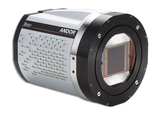
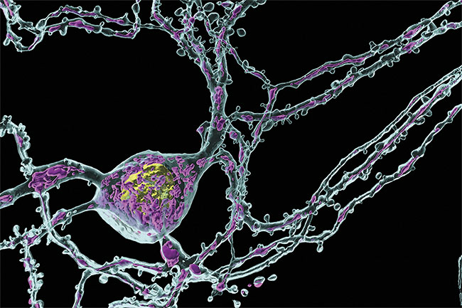
Such techniques result in low signal levels, meaning that high-sensitivity cameras are required to support studies that are at the forefront of how we understand cell biology. sCMOS cameras meet the technical demands of many of these imaging experiments. Compared to slower CCD-based cameras, sCMOS cameras’ high sensitivity combined with fast speeds over wide fields of view (Figure 2) make them well matched to dynamic live-cell imaging. This enables abilities such as capturing neurons firing as part of large networks (Figure 3), viewing large tissue sections, or studying cell development in the context of the full organism.

Figure 2. A large-area scientific CMOS
(sCMOS) camera. Courtesy of Andor
Technology.

Figure 3. An image of a neuron taken with an Andor sCMOS camera and a confocal microscope
and rendered in Imaris software for analysis. Courtesy of Aubrianna Decker and Daniel Virga.
However, exceptions remain when using sCMOS cameras for certain niche, yet important, imaging experiments. When light levels really become limited, at depth, EMCCD cameras are often the only ones that are sensitive enough to study processes at the single-molecule level, for example.
Detecting luminescence
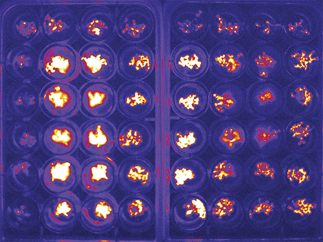
Not all biological processes happen at a fast pace. Capturing slower processes, such as luminescence, places different demands on the imaging sensor. Luminescence is the emission of a light signal from a chemical reaction; therefore, no illumination of the sample is required. Detecting luminescence involves collecting weak signals over extended durations (Figure 4). Provided that the background noise is kept to a minimum, a very high signal-to-noise ratio can be achieved, making it possible to reveal small changes in processes. Examples include gene transcription studies, or experiments involving the circadian rhythm processes of plants that would be difficult if not impossible to capture using other techniques.

Figure 4. Luminescence studies in two sets of 24-well plate of the model plant
Arabidopsis. Courtesy of the Liu Lab.
The key features needed for an imaging detector for such experiments are the optimal collection of the weak signals emitted from the specimen and the lowest possible sensor-related noise. Over extended exposures, dark current is the dominant noise source. Thermoelectric deep cooling of the sensor using air or liquid can limit the generation of dark current. Deep-cooled CCD cameras are the best-suited imaging cameras for use over extended exposures. These models combine high quantum efficiency with large pixel sizes to maximize the collection efficiency of weak signals. Their slow readout rate, which is a disadvantage for dynamic cellular and physical events, can be a benefit at longer exposures.
Although the read noise of deep-cooled CCD cameras is higher than that of sCMOS cameras, the dark current of CCD cameras is orders of magnitude lower. Read noise is the dominant noise at short exposures, with dark current making a negligible contribution. Once exposures increase to the durations required for luminescence experiments, dark current begins affecting the signal readout. Therefore, deep-cooled CCD cameras, which are much too slow for faster imaging experiments, are ideal for these slow, long-exposure luminescence experiments due to their very low dark current.
Looking to the skies
Early imaging sensors were often small and had low pixel counts, which were limited in part by the speeds and sensor fabrication techniques of the time. Sensor technology has since been developed to allow for considerably larger sensor sizes with many small pixels, and to run at high speeds. For microscopy, the field of view is inherently limited by the microscope objective lenses and supporting optics, setting a practical limit on sensor sizes. Outside of these constraints, a need remains for much larger-area imaging cameras.
One example that is driving larger sensor sizes is the tracking and observation of space debris. With an ever-increasing number of floating objects being created by jettisoned rocket booster stages and other sources, debris must be tracked to prevent collisions with valuable satellites in the vicinity. Having a much larger sensor area allows for greater areas of sky to be surveyed at any one time. Large-area, deep-cooled sCMOS cameras are now available that enable more fast-moving objects to be detected and analyzed, including their speed and trajectory.
Large-area, deep-cooled CCD cameras are also available that may not offer the imaging speeds necessary for fast-tracking applications, but they do allow vast areas of the sky to be studied, as is required for the sky surveys used by astronomers. These cameras provide the low dark current level required to permit the long exposure times that are needed when capturing faint signals from distant celestial events or bodies. A complementary fast sCMOS camera can be used as a guide, acting as a tracker for the main camera, to compensate for the movement of the Earth relative to the source during the exposure.
Quantum imaging and camera choice
Quantum research has moved beyond physics, with key applications in computing, information processing, and biology. Quantum imaging affords unique insights that are not possible to achieve from classical imaging. For example, the measurement of photon pairs or photon coincidence is important when studying quantum behavior, such as ghost imaging and quantum holography. Initially, raster scanning-based approaches were popular for performing quantum imaging. More recently, researchers have employed camera-based solutions.
EMCCD cameras are highly valued in single-photon or single-molecule imaging experiments, and increasingly in quantum research as well. Offering single-photon sensitivity, low noise, and high quantum efficiency in the broadband visible range, EMCCDs can capture most single-photon events. For certain applications, single-photon avalanche diode arrays are used for quantum imaging, typically having lower quantum efficiency than EMCCDs but offering faster frame rates.
Future possibilities
One camera will likely never be optimal for all imaging applications, given the wide range of parameters that applications can require. The most suitable camera technology must be selected based on specific experimental requirements. Although many of the recent developments in imaging cameras have centered around CMOS-based sensor architecture, some niche applications are still better matched to CCDs, even while they may be viewed as older technology. Despite sCMOS and CCD sensors being well developed, future innovation of these core technologies may assist users in increasingly complex experimental techniques and analysis procedures.
Future development potential for
sCMOS includes an extended near-infrared (NIR) response, which would enable applications in biological imaging as well as in other areas, such as material sciences and astronomy. Currently, sCMOS sensors can achieve 95% peak quantum efficiency in the visible regime. Extending the quantum efficiency response to the NIR has many benefits. These include facilitating additional biological tags, without risk of overlap between spectra, to concurrently study more components in a biological system. Additionally, imaging in the NIR region of the spectrum means less scattering and thus better compatibility with deeper tissues.
High-temporal-resolution or 3D images — and longer experiment durations — mean more image data processing and analysis. Software is vital for helping to manage vast volumes of image data, and data management solutions are becoming more and more common.
Overall, simultaneous advancements in both hardware and software are most likely to offer improved imaging and analysis experiences for users, in addition to the broadening range of applications of sensor technology.
Meet the authors
Alan Mullan, Ph.D., is a product specialist for microscopy cameras at Andor Technology. He keeps in touch with the imaging needs of researchers in many areas of research, as well as with the latest developments in imaging sensor technology. After academia, Mullan spent time working in the medical diagnostics, food, and pharmaceutical industries, in applications and technical roles, before joining Andor; email:
[email protected].
Aleks Marsh, Ph.D., is the technical author and copywriter at Andor Technology. She maintains specifications and documentation for the Andor product range, keeping up to date on camera technologies and applications. Marsh completed her doctorate in chemistry at the University of Bristol in 2018. During her doctoral research in the field of aerosol science, she used single-particle techniques to improve understanding of the impact of aerosols on human health and climate; email:
[email protected].