Full company details
Thorlabs Inc.
 43 Sparta Ave.
Newton, NJ 07860
United States
Phone: +1 973-300-3000
Fax: +1 973-300-3600
Partners Lay Groundwork for Scalable Quantum Integrated Photonics
Photonics Spectra
Aug 2025Aeluma, in collaboration with Thorlabs, has demonstrated wafer-scale integration of the nonlinear optical material aluminum gallium arsenide (AlGaAs) onto CMOS silicon photonics-standard 200-mm diameter wafers. According to Aeluma, the demonstration and method could accelerate the adoption of quantum computing and communications at commercial scale.
The nonlinear optical material enables entangled photon pair generation and modulation, key building blocks for quantum photonic systems. Compared with other materials such silicon nitride or lithium niobate, AlGaAs offers significantly improved efficiency for next-generation quantum photonic circuits, according to the collaborators.
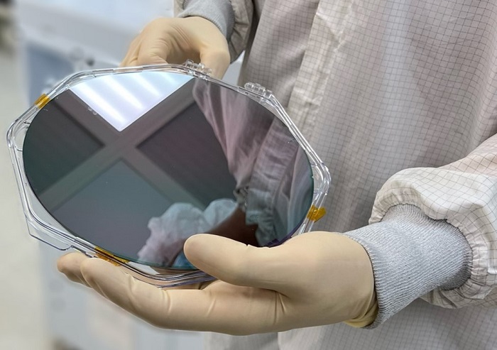
A 200-mm wafer manufacturing method developed by Aeluma and Thorlabs could provide an avenue to manufacture quantum photonic circuits on silicon in a scalable fashion. Courtesy of Aeluma.
“Quantum integrated photonics requires different materials to control quantum states. High-performance materials, including aluminum gallium arsenide, lithium niobate, or barium titanate, are not traditionally compatible with large-scale, 200-mm and 300-mm silicon photonics,” said Jonathan Klamkin, CEO and director of Aeluma. Scalable heterogeneous integration techniques are needed to bring these materials together, he said.
According to Garrett Cole, manager of Thorlabs Crystalline Solutions (TCS), the collaboration sought to combine the core strengths of the companies’ respective teams, which are both located in Santa Barbara, Calif. Aeluma, he said, produces high-quality epitaxial compound semiconductors at wafer sizes up to 300 mm. TCS has pioneered direct bonding processes for novel III-V-based compound-semiconductor-on-insulator materials, such as AlGaAs and indium gallium phosphide on oxidized silicon.
“Our aim was to bring these capabilities together to demonstrate high-performance compound semiconductor-on-insulator wafers at commercially-relevant scales,” Cole said. “There have been several demonstrations of smaller R&D-level solutions, but this is the first, to our knowledge, of a demonstration that is truly scalable.”
According to the collaborators, the work provides opportunities for quantum systems developers, as it provides their desired performance alongside an inherently mature manufacturing process. Broadly, it also showcases the potential to integrate mature III-V materials, which, Cole said, offers high intrigue given the high-performance properties of these materials for both quantum and classical applications.