JEAN BRUNELLE, TELEDYNE DALSA
Long-wave infrared (LWIR) imaging, also known as thermal imaging, has played a critical role in the defense and security market for decades because of its ability to detect warm (or live) objects independent of ambient lighting. Recently, advances in detector fabrication and lower costs have made LWIR imaging more accessible for consumer and industrial markets.
LWIR detectors do not see scattered and reflected visible light; they are mainly responsive to infrared heat emitted from objects themselves. One way to experience this deep infrared light is with the outdoor heaters found on many terraces or the red heat lamps that keep trays of food warm in a restaurant. They heat skin (or food) by emitting a large quantity of infrared radiation.
An LWIR sensor can indicate where and in what quantity heat radiation is emitted. This offers two distinct advantages: The scene becomes independent of lighting conditions and the sensor is able to easily identify any type of heat-generating body. This last advantage has long made LWIR sensing a critical enabling technology for modern warfare.
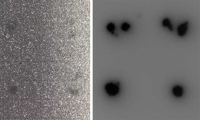
Visible (left) and LWIR (right) images of glue drops on a piece of foam. Courtesy of Teledyne Dalsa.
The other applications for this technology generally fall under one of two categories. Pure imaging applications are dependent only on the visibility of heat distribution. Radiometric applications rely on the ability of specially calibrated LWIR cameras to return the absolute temperature of objects present in the scene. Some information about the nature of the object’s surface finish is required since this determines how much radiation it reflects or absorbs.
Thermal imaging applications based on pure imaging are many — and expectations for this number will only grow. Locating hot spots in printed circuit board manufacturing and the detection of water and insulation breaks are well-known uses for LWIR imaging. Devices for these types of inspections have been available commercially for decades. Two of the more uncommon examples are glue drop detection and cowhide inspection.
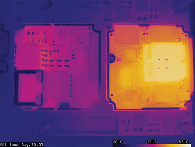
LWIR images of camera boards show circuit inspection. Courtesy of Teledyne Dalsa.
Consider a glue drop inspection application that tries to detect and measure the position of newly placed glue drops on a product. The problem is that the glue in question is completely transparent and the part that it sits on (the background) is very dark, so the drop is difficult to resolve and image in traditional visible imaging. Luckily, liquid glue possesses a very different thermal dissipation and emissivity (the surface property governing LWIR emission from objects) than the background object. This makes it easy to detect as a clearly defined black spot in a thermal image.
In the case of cowhide inspection, the goal is to find “hard spots” inside newly processed hides. These hard spots are impossible to see in visible light and currently are detected manually by patting the whole surface of the hides. To automate this process, it is necessary to gauge the density of the material. This is a case where detection is not directly visible in LWIR at a steady state. But if the temperature of the hide is raised and then cooled passively, the differences in density are revealed as differences in temperature after a certain amount of cooling. These types of indirect inspection applications are many. If a defect can be detected by observing heat transfer or heat distribution, it can be resolved with LWIR imaging.
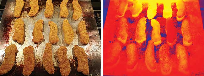
Visible (left) and LWIR (right) images of chicken strips. The LWIR image shows the variation in temperature. Courtesy of Teledyne Dalsa.
Radiometric applications of LWIR imaging can be a great asset for industries such as food and material transformation because it offers the capability to measure, from a distance and without physical contact, the temperature of any shaped object at random locations. This allows for greater coverage in process control, as well as yield loss reduction. A chicken nugget factory, for example, might want to validate the temperature of all of its products when coming out of the oven. With a properly calibrated camera, all that is required for accurate measurements is to input information about the target object’s surface finish (emissivity) and the ambient conditions (humidity and temperature).
For years, the need to actively cool the detector with liquid nitrogen or other means drove up the cost and made cameras bulky. This was a major deterrent to the use of LWIR imaging in industrial settings. In the mid-1990s, Texas Instruments introduced LWIR technology to the commercial market with a barium-strontium titanate (BST) sensor1,2. The ferroelectric device was later abandoned after first rounds of optimization because it had about 2.5× less signal-to-noise ratio than the alternative that was investigated in parallel: vanadium oxide. Because both technologies were originally developed by the military, after they abandoned BST in favor of VOx, BST was quickly replaced in most applications, as it fell behind in performance because of lack of research.
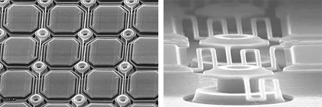
Long, thin legs (right) suspend IR-sensitive elements above the sensor substrate (left) in a bolometer. Courtesy of Teledyne Dalsa.
Both BST and vanadium oxide (and later amorphous silicon) microbolometers3 were introduced as alternatives to cooled optoelectronics in an effort to reduce the price and size of these detectors. A bolometer (from the Greek bole, or beam of light) is a temperature-sensitive resistor. For imaging, an array of microbolometers are used. A majority of them are exposed to incoming radiation, with several columns of nonexposed or “blind” resistors providing a baseline reading.
By reading out and integrating the changes in these exposed resistors when compared to nonexposed resistors, a thermal image can be recreated. This measurement is made through long, thin support legs that suspend the resistor above the sensor substrate. Isolating the resistor in a vacuum and away from contact with any surface maximizes the temperature change for a change in flux (the rate of transfer of particles, or energy, across a given surface).
A main challenge with using microbolometer-based detectors is that each measurement is a comparison between two elements (the exposed resistor and the shielded resistor); variations in the exact resistance value of these elements across the array leads to high fixed-pattern noise (FPN) in the image. Measuring such small differences in resistors, the FPN effect is actually comparable to the pixel response, causing the raw image from the detector to look noisy in most cases.
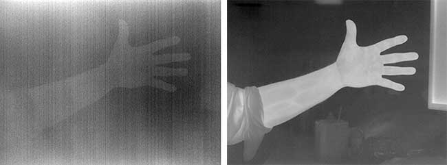
An LWIR image of a person’s arm before (left) and after (right) fixed-pattern noise correction. Courtesy of Teledyne Dalsa.
Since this difference per pixel is mostly offset based, it is possible to correct it by using a simple shutter. With a shutter in front of the detector, the difference in every pixel to the target is measured and a correction applied, as the uniform surface provided by the shutter should output the same pixel value for all pixels. The FPN correction results in a much cleaner thermal image.
Unfortunately, however, the correction is highly dependent on the current sensor temperature. This dependence drives the need to have an integrated mechanical shutter inside the camera, which increases the complexity and cost of the camera. For this reason, LWIR imaging companies have been working on a shutterless correction.
In theory, since the amount of correction to be applied to any given pixel is determined by the current sensor temperature at the substrate level, it should be possible to predict and store into memory the correction to be applied, even as the camera temperature changes. With the increase in available computational power in embedded electronics and integration of these kinds of corrections into ASIC or FPGA designs, more and more of these shutterless alternatives will be available on the market. Since the shutter action blocks the optical path for a certain time, thus obstructing the view of the camera for that time, shuttered cameras are difficult to use in continuous inspection applications where dropped frames are a problem. This is also the case for most surveillance/monitoring and detection/avoidance systems, such as on an autonomous drone. Shutterless cameras are a solution to these problems.
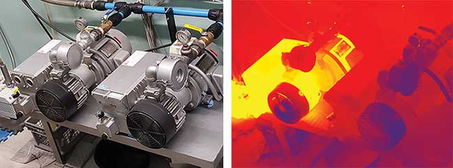
Visible (left) and LWIR (right) images of two water pumps. The pump that is on is warm, and thus shows up yellow in the LWIR image. Courtesy of Teledyne Dalsa.
To achieve any kind of significant response from this type of detector, the sensitive elements need to be encapsulated in a high-vacuum package so that it does not leak or transfer its heat to the environment through convection. The “old” way of doing this is referred to as die-level packaging (DLP) and involves dicing the element array and packaging them into a vacuum capsule under a window individually.
This process is costly and greatly increases the required package size for a given pixel size/resolution. Another strategy being developed to reduce cost and size is called wafer-level packaging (WLP). This involves bonding a full wafer of bolometer arrays onto a wafer of vacuum capsules with integrated windows. The WLP process is much more demanding at the microfabrication level, but the gains in terms of price and size per die are well worth the added trouble. The improvement goes a long way toward making these cameras accessible at a price where cost-reduction-driven inspection systems become viable. It also eventually will permit mass production of bolometers on a whole new scale and at a detector size that will enable another wave of integration into mass market devices such as cars, drones and cellphones.
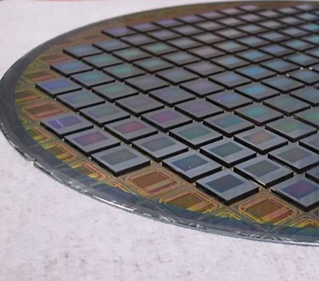
Wafer-level packaged microbolometers. Courtesy of Teledyne Dalsa.
Whether through direct observation of heat distribution, indirect observation of heat movement and variation, or through absolute temperature measurements, thermal cameras are bound to take a bigger place in the automation/inspection expert’s toolkit in the future. The specific strengths and challenges of such a technology do not make it an all-around solution for inspection. For specific situations where visible light fails to provide meaningful insight or an understanding of the properties of the target being inspected, thermal cameras present a valid alternative. With the price and size of these devices decreasing steadily, they will inevitably enter the machine vision market in one form or another.
Meet the author
Jean Brunelle is a technical leader in sensor integration at Teledyne Dalsa. He develops new image correction and calibration algorithms, as well as qualification and production tests for the company’s visible and LWIR lines of digital cameras. Having received a bachelor’s degree in engineering physics and a master’s in surface chemistry, Brunelle’s focus for the last few years has been on microbolometer-based LWIR cameras, trying to introduce high-quality, shutterless, low-cost cameras to the market. Most recently, he was involved in the development and testing of Teledyne’s very own WLP microbolometer and its integration into a shutterless camera. For more information, visit www.teledynedalsa.com; email: [email protected].
References
1. D.A. Jackson (1995). Detector material for uncooled thermal imaging devices. Patent US 5079200.
2. H.R. Beratan and C.M. Hanson (1997). Monolithic thermal detector with pyroelectric film and method. Patent US 5602043.
3. R.A. Wood (1995). Use of vanadium oxide in microbolometer sensors. Patent US 5450053.