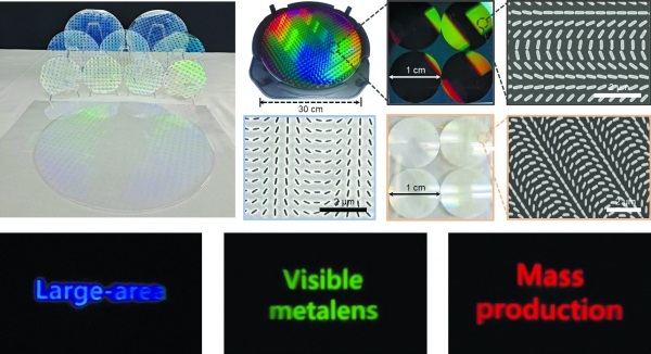
POHANG, South Korea, May 25, 2023 — Researchers at Pohang University of Science and Technology (POSTECH) have demonstrated the mass production of metalenses for visible light wavelengths on a wafer scale. The researchers combined photolithography and nanoimprint lithography. Where photolithography uses light to pattern a substrate, nanoimprint lithography uses a stamp with nanosize patterns to print patterns onto a substrate.
According to the researchers, metalenses offer a promising alternative to conventional bulky refractive lenses due to their submicron-scale thickness and light-modulating performance. Limitations continue to affect existing fabrication techniques, however. These include high cost, low throughput, and small patterning areas.
Through the synergy of the two existing lithography techniques, the researchers said that the study represents a step forward for the commercialization of metalenses. The work was selected as the inaugural project of the POSCO-POSTECH-RIST Convergence Research Institute, an industry-academia consortium funded by the South Korean steel company POSCO.
The researchers first created a single pattern using electron beam lithography, and they then replicated the pattern using deep-ultraviolet argon fluoride photolithography to create a 12-in. master stamp. Using the stamp and nanoimprint lithography, the researchers successfully produced metalenses with a 1-cm diameter at high speed.

POSTECH researchers achieved mass production of metalenses capable of transmitting light in the visible spectrum. Courtesy of POSTECH.
Conventional nanoscale structures based on nanoimprint technology have traditionally had low refractive indices, resulting in low efficiencies of around 10%. This has required significant costs to improve their efficiency. In the recent work, the researchers improved the efficiency of the lens up to 90% by coating the lens with a thin layer of titanium dioxide of about 20 nm.
According to the researchers, the approach allowed them to fabricate hundreds of centimeter-scale metalenses using a thinly coated high-index film to enhance light confinement. This, they said, resulted in a substantial increase in conversion efficiency.
As a proof of concept, the researchers then demonstrated the practicality of metalenses by creating lightweight virtual reality devices capable of displaying images in red, green, and blue.
The study was financially supported by POSCO, the Samsung Research Funding & Incubation Center for Future Technology, and the National Research Foundation of Korea.
The research was published in Nature Materials (www.doi.org/10.1038/s41563-023-01485-5).