
Surface Analysis Reaps the Benefits of Increasingly Automated Workflows
Classical techniques remain in use for surface measurements — and their efficacy is on the rise, due to the adoption of sophisticated data collection and analysis tools.
By Joe Kuczynski
Engineers and end users deploy optical metrology methods for surface analysis at points up and down the optical design value chain. In many instances, these optical test and measurement protocols represent the most effective approaches to gauge surface parameters — from smoothness or roughness to reflectivity, to hydrophilicity or hydrophobicity. Such qualities are highly consequential not only during the component design and manufacturing stages, but also throughout system and product rollout.
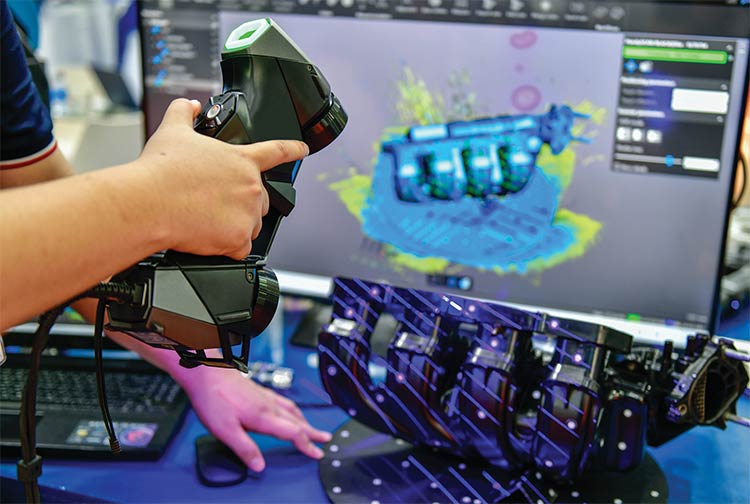
Courtesy of iStock/MJ_Prototype.
Both methods and applications characterize the evolution of optics-based surface measurement technology.
Noncontact methods in use today can deliver precise results in real time, with advanced systems providing >10 million
measurements at high resolution. Techniques for analyzing complex and sophisticated surfaces — such as aspheric and freeform optics — are also soaring, in lockstep with the applications that these components enable.
Another major shift is underway: External technology drivers are bringing previously unattainable levels of functionality to surface measurement.
Advancements in the fields of automation and AI are improving the speed of both data collection and processing. Increasingly, today’s systems are exiting experimental environments and entering factories and warehouses.
Yet even as these technologies move toward the mainstream, the utility they offer cannot fully compensate for the need to align the right technique with a given application. No single system can deliver optimal results for all jobs, and selecting the best system for a given task requires companies to set benchmarks for parameters beyond just accuracy and speed. Especially in manufacturing,
considerations of cost and system implementation are imperative to avoid bottlenecks on the production line.
As industry continues to demand more data to be gathered and interpreted in shorter times, these demands are pushing the bounds of surface detection and
measurement. Aided — though not replaced — by robotic systems and deep learning, existing methods are reaching new levels of performance. Approaches based on laser triangulation, chromatic confocal measurement systems, and optical camera imaging are among those finding sustained use amid this paradigm shift in surface and materials analysis.
A system for every job
Determining the distinct characteristics of a surface or material is essential to ensure accurate measurements and
analyses. Visually, users may be able to make cursory determinations of surface texture, size, and shape. However,
gathering information on other parameters, such as material composition and depth, commonly requires the use of sensors. Plus, factors such as the temperature at which the surface material(s) will be measured and the distance from the surface at which the measurement must be taken blur the lines between the challenges of precision surface analysis and the limitations of the techniques used to perform it.
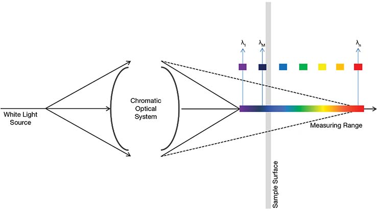
A chromatic confocal measurement system as it directs white light through a filtering optical component and onto the surface of a material. The light is separated into wavelengths and reaches the sample surface as a continuous, wavelength-encoded array of focal lines. Measuring these wavelengths provides highly accurate surface analysis data.
Lasers are at the core of many widely used optical surface analysis techniques. Laser triangulation, whether in point
or line form, can deliver precise measurements in the micron range. The adjustability of the triangulation angles also enables users to achieve an ideal combination of range and resolution, while high-speed processing makes this a favored technique for inline measurement and process control. Additionally, laser triangulation can be performed at various distances from the surface under analysis, ranging from a few millimeters to several meters away.
Still, laser-based systems have evident shortcomings: Surface texture and sharp edges can be problematic because these features may cause speckle and edge artifacts that taint the data. “Laser-based measurement methods are great for certain applications, but they are not very good at shiny surfaces, for example. And the resolution you can get from [laser-based] methods is limited by the optics and by what you can actually do with the laser source itself,” said Simon Harding, technical director at Scantron Industrial Products.
“You can see features smaller than the width of a laser line or laser point, but you lose fidelity, and it is difficult to infer what you get from the scan.” Laser-based methods based on the principle of triangulation, according to Harding, also suffer from shadowing and occlusions.
According to Yves Surrel, founder of Wyse Light — a company specializing in the optical measurement of reflective
surfaces — modern machining and
polishing techniques can make even the most complex shapes reflective. This necessitates dedicated metrology systems that can keep up.
“Surfaces of complicated shapes are no longer a problem,” Surrel said. “Now, we are seeing a rapid emergence of freeform-based reflective imaging systems that are smaller and lighter than traditional solutions. It is clear that accurately measuring the shape of reflective surfaces has
become a crucial issue for imaging systems manufacturers, for example.”
Chromatics
In the context that Harding cites, chromatic sensing may provide a solution. By shining white light through a fiber optic lens that splits it into a vertically projected spectrum, a user can then measure the returning reflected light. Meanwhile, an analysis of the dominant wavelength for the spectrometer “tells” the system the necessary information on displacement. Importantly, the top-down vantage point also eliminates the triangulation issues that laser systems face.
Chromatic systems can be used on most surface types, regardless of how reflective or transparent they are, Harding said. “With the chromatic, you can get down to the vertical resolutions in the nanometer range quite easily. The sensors themselves are at a fundamental level capable of resolving features hundreds of times smaller than the best laser systems. We use these often for surface measurements in challenging environments.”
Higher-end chromatic systems often carry a greater cost than the equipment needed for laser triangulation setups, and these systems also fail in many instances to reach the same operating speed.
As mentioned, the capabilities of human vision alone are sufficient for
surface defect detection in some cases.
In others, the use of optical imaging
cameras serves as a bridge between human vision and laser-based metrology
techniques. For example, a user may deploy an optical camera or a combination of cameras to locate a problem area, and then use a laser scan to precisely qualify the defect.
A major consideration in using optical
imaging cameras for surface defect analysis involves the potentially large volumes of data that must be analyzed. The first wave of challenges arises from the environment in which the images are captured. A laboratory environment, for example, is likely to be interactive, with researchers and engineers constantly adjusting parameters and controls. As a result, camera sensor customization is often necessary to deliver as much data as possible. Production lines, meanwhile, prioritize consistency and repeatability.
Even when a system adequately satisfies the requirements for data gathering, processing the collected data can become a bottleneck. The right software and
system combination enables the optical
imaging mechanism to provide the needed results.
According to Harding, visually capturing surface information can also extend to capturing a function as it is performed. Additionally, capturing data on who is doing the work can be important for traceability.
“We also have to capture things like the whole scanning setup of the system at the time the scan was done, because some of our customers work in areas where they might need to keep records for the whole lifetime of products, which could be
25 or 30 years,” Harding said. “The duck
swimming on the surface of the pond yields very different information than the duck underneath the water.”
According to Harding, even if delivering usable information on surface characteristics is the goal, how the surface functions in real-life situations is crucial information to provide to end users and customers.
Smart systems reshape the landscape
Factories are implementing more automation than ever before, often in the form of sophisticated automated, robotic, and AI-based systems. The use of digital twins, or virtual representations of a product or process, offers tremendous value in connecting digital and physical aspects on the production line. The benefits are tangible in predictive maintenance, reduced downtime, cost savings, and more.
Groups including ZEISS, which provide customers with inline metrology
systems for coating analysis of large areas, are among the companies that now rely on smart systems. The involvement of these systems is only expected to grow, according to Chris Hellwig, product manager of thin film at ZEISS Spectroscopy. “Some of our target applications are driven by smart systems,” Hellwig said. “Our detectors become ‘smarter’ with each new generation — the optical functions, electronics, evaluation, and communication grow together in smart detectors. This makes the integration in existing and new production lines much easier.”

Deflectometry systems can be used to make 3D surface shape measurements with a high level of accuracy. This technique uses patterning to determine the shape of reflective surfaces. Courtesy of Wyse Light.
Erik Novak, vice president of 4D Technology, echoes the importance of integrating smart capabilities into commercial measurement systems. “Automation significantly increases throughput with higher sampling rates and accuracy with the robotics’ precision, and when paired with appropriate optical sensor technology, delivers gauge capability.”
On a macro scale, the integration of AI and smart functionality is a bona fide trend in industry. “You’ve got, at the moment, a bit of a revolution in factories and manufacturing,” Harding said. Smart
systems have advanced far beyond merely interpreting and acting on generic statistics. With the right software solution and as part of a system tailored for its
specific environment, a test and measurement protocol can deliver unprecedented detail on surface form and finish. This means that such optical metrology
systems can now also offer more data for an AI-driven system to ultimately process.
According to Harding, this trend, among other applications, is blossoming in additive manufacturing workflows.
“A lot of companies are doing a lot of work in trying to work out how to use a 3D printer in the laser sintering process, for example,” Harding said. Metal bashing and welding are hardly new or novel applications. Additive manufacturing, though, represents a newer frontier. The result is a lack of fully mature processes and an absence of data about them.
As complete production lines get smarter, so too do the optical system
elements. AI-enhanced measurement sensors are now used to capture vast amounts of data in real time. Scantron, for example, uses AI in its systems to locate and classify defects, with the aim of improving how data is contextualized and used to predict the performance of measurement systems.
Added precision across all manufacturing steps and processes means that even production lines that are comparatively straightforward — for example, those used to analyze the surface of a can of soda — can produce less waste and deliver cost savings.
Limitations on surface analysis
Some of the challenges that continue to hinder surface analysis quality are equipment- or machinery-based. For example, in applications that use optical (laser) scanning, the size of the measurement (scan) head remains an obstacle. Larger systems struggle to fit into smaller spaces. And as the bounds of miniaturization continue to stretch, some systems are unfit for the very types of applications they enable.
“If you want to look inside a small
aperture or inside something, it can be quite challenging. And now, with the advancements in 3D printing, people are building all sorts of crazy shapes and crazy geometries,” Harding said. “Getting your sensor in for inspection is getting harder and harder.”
Still, according to Harding, designers are constantly developing sensor solutions to meet the demands of current application challenges. “But there is always going to be a limit to the size of a lens, or the size of a laser, or the size of the optics. And that is going to be a bit of a bottleneck or an issue in some inspection techniques,” he said.
Other surface evaluation issues derive from the shapes and material complexity of surfaces.
“Surface roughness measurements [present] some more challenging issues, particularly when looking to use one system to measure a large variety of machined surfaces and reflectivities, which can range from mirror-smooth to sandpaper-rough,” said 4D Technology’s Novak.

Offline measurement systems offer accuracy down to the micron level, a critical feature for devices used in applications such as defect detection in metals and other materials. Courtesy of Scantron.
When evaluating optics themselves, measuring aspheres and freeforms interferometrically can be time-consuming and costly if there is a need for tailored computer-generated holograms to align the measurement setup. Current optomechanical systems can be deployed for freeform measurements, but costs can be prohibitive.
According to Wyse Light’s Surrel, a fully reflective or transparent material still necessitates additional considerations. “Lenses, when illuminated, will show internal reflections on the back of the surface, which may lead to intractable measurement problems when the reflections on both front and back surfaces overlap,” he said.
Surface texture can also lead to inaccurate measurements from systems. Rugosity, for example, which is often a physical surface trait of blanks and/or semifinished surfaces, may impede a system’s ability
to deliver an accurate measurement.
A window to the future
Measurements that once required hours
or even days of manual work are now completed in minutes or even seconds, with more accurate results. High levels
of system durability are providing
manufacturers with critical surface
measurement data, even in noisy and
active environments.
Now, as AI, deep learning, and automation burgeon, improved techniques
delivering improved results are apt to find their place in all use environments.
Imaging for Accuracy
Optical cameras are not the only imaging instrumentation used for precision surface analysis. Particularly at the nanoscale, optical microscopy, especially brightfield microscopy, offers a relatively simple technique for illuminating samples. The method is also cost-effective and highly accurate. Hand-held devices, such as those from 4D Technology, use polarized structured light to obtain 3D measurements. Systems such as the company’s 4D InSpec are used to image defects such as pits, particles, dings, and scratches. Smart software automatically flags these abnormalities.

Manufacturers use 3D hand-held optical gauges with supporting software for fast, versatile, and accurate measurements. These devices can overcome vibration issues and enable companies to save time by taking the measurement to the part. Courtesy of 4D Technology.
Published: September 2025