With the development of a single-layer, blue-emitting OLED, researchers at the Max Planck Institute (MPI) for Polymer Research demonstrated that one-layer OLEDs can achieve a performance level comparable to commercial OLEDs with multiple layers, while simplifying OLED design, fabrication, and analysis.
Early OLEDs had a simple device structure. A semiconducting layer was sandwiched between two electrodes. Holes were injected into the organic semiconductor layer via the anode, and electrons via the cathode. Since then, considerable efficiency gains have been made by increasing the number of functional layers in OLEDs.
However, multilayer OLEDs are complex to design and fabricate. The need for additional fabrication steps can drive up production and manufacturing costs, and the multiple heterojunctions in multilayered OLEDs can give rise to energy barriers that lead to voltage losses and device degradation. The production of blue OLEDs is especially challenging.
The MPI team showed that, instead of several layers, a single active layer that is responsible for light emission, sandwiched between two ohmic contacts, is sufficient to obtain a highly efficient blue OLED. The material used in the single active layer prevents defects, such as water and oxygen, from affecting the OLED.

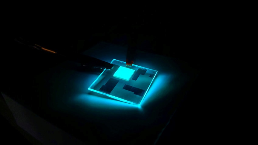
Researchers at the Max Planck Institute developed a blue OLED consisting of just one layer. The new material concept demonstrated efficiency comparable to commercial OLEDs with multiple layers. Courtesy of the Max Planck Institute for Polymer Research.
The single-layer, blue-emitting OLED consists of a layer of a thermally activated delayed fluorescence emitter blended with a host. The emitter and the host are blended in equal ratios.
This layer is sandwiched between a polymer poly(3,4-ethylenedioxythiophene) polystyrene sulfonate (PEDOT:PSS)-perfluorinated ionomers (PFI) hole contact and a metal top electrode, without any additional interlayers. The presence of a host in the emissive layer of the OLED eliminates the need for an organic tunneling interlayer for ohmic electron injection.
The researchers demonstrated that a blend film containing PEDOT:PSS and PFI can provide ohmic hole injection into high-ionization energy organic semiconductors, allowing for a simplified, single-layer OLED with 27.7% external quantum efficiency and low operating voltage, with minor roll-off at high brightness.
Due to optical losses at the interfaces, which are present in every OLED, about 27% of the light is emitted to the outside in the single-layer OLED. This value is competitive with the existing commercial OLEDs that use a multilayer material system. The multilayer sandwich structure, comprising as many as seven layers, allows efficiencies of light emitted to the outside that are between 20% and 30%.
Using optical outcoupling simulations, the researchers demonstrated that the single-layer OLED can achieve close to 100% internal quantum efficiency, establishing that additional charge- and exciton-blocking layers are not needed in a single-layer OLED with ohmic contacts. The results show that highly simplified, single-layer OLEDs with zero electrical losses are a feasible alternative to multilayer devices.
Currently, an OLED TV screen requires about six million OLEDs — three OLEDs for each pixel. Making OLEDs easy to manufacture and energy-efficient is necessary to control manufacturing costs, as well as the cost of the electricity needed to operate the OLED device. Blue OLEDs, which are used in smartphones, TVs, and other devices, continue to be challenging to manufacture using traditional methods.
The researchers’ approach to producing OLEDs demonstrates that a simple device architecture using a minimal number of materials and coating steps can rival the performance of current multilayer OLEDs. The design for the new OLED could provide the foundation for the development of efficient, fully solution-processed, single-layer OLEDs.
“With our material system, efficient blue OLEDs could also be produced from solution in the future,” Gert-Jan Wetzelaer, who led the research, said. “This means that manufacturing then no longer involves a multistep process and complex evaporation equipment, but such OLEDs can also be printed in the best-case scenario.”
In addition to offering advantages from the perspective of device design and fabrication, the simplified, single-layer OLED structure could be useful for developing a better understanding of OLED device physics. This is complicated to do with multilayer architectures, due to the presence of multiple materials, and of multiple heterojunctions and their associated energy barriers with charge-transport and barrier-height parameters that are rarely understood well enough to analyze in a meaningful way.
The research was published in Advanced Materials (www.doi.org/10.1002/adma.202300574).