Thanks to innovations with heterogeneous material integration and multiphotonic layer stacking, silicon photonics will drive optical solutions to high volumes and low costs.
Christophe Kopp, Ségolène Olivier, and Stéphane Bernabé, CEA-LETI
Silicon photonics is widely considered a key enabling technology for further development of optical interconnect solutions needed to address growing traffic on the internet. From the first submarine optical cable to the fiber-to-home deployment to the proliferation of data centers, light has served as the ultimate medium for high-speed optical communications for more than 20 years. Compared with copper wiring, optical interconnect can work over long and short distances with low latency, low energy consumption, and high-speed, leading to end-to-end network paths. For this reason, optical links are being implemented into modules at many internet network levels including server, switch, network-attached storage, clients, and others.
In this context, silicon photonics is a relevant technology to drive optical solutions to high volumes and low costs. Indeed, several platforms have been developed as photonic integrated circuit (PIC) technologies — glass, plastic, silica-on-silicon, indium phosphide, lithium niobate, and silicon-on-insulator (SOI). These platforms exhibit a rather uneven integration capability level, depending on the optical mode confinement and the possibility to implement passive and/or active functions. In this quest for higher integration, silicon photonics on an SOI platform provides a wide panel of benefits.
Optoelectronic integration
Thanks to the high index contrast between silicon and oxide, small footprint circuits can be designed with submicron-mode field diameter and few-micron waveguide bend radius. Moreover, silicon material is amenable to optoelectronic integration, as it is both semiconducting and transparent in the telecom wavelength domain. Silicon photonics is also highly scalable to increase the bit rate per channel on the same chip by implementing wavelength multiplexing and advanced modulation formats. In addition, the use of microelectronic CMOS fabrication lines for silicon PICs allows low-cost mass production. For instance, fabrication on 200-mm- or 300-mm-diameter SOI wafers enables high-volume performance measurement with wafer-level automated testers (Figure 1).
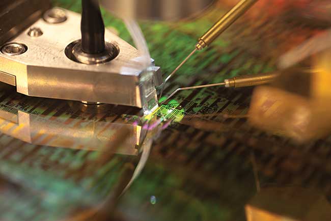
Figure 1. Wafer-level automated testing of a PIC.
In order to solve electrical interconnect limits in data centers and supercomputers, silicon photonics has attracted increasing investments to address the requirements of next-generation optical transceivers in small form factor modules for optical interconnects ranging from metropolitan transmissions to data center short interconnects and high-performance computing. There are many advantages to silicon PIC-based transceiver modules compared with legacy technologies (VCSELs or InP-based modules). Among them, silicon photonics enables the integration of a large number of passive and active optical functions, such as, modulators, wavelength- and polarization-management devices, photodetectors, and even hybrid laser sources, on a single chip.
Metro networks, inter- and intra-datacenter interconnects
Silicon photonics components can be integrated in complex photonic circuits to transmit and detect complex modulation formats, including polarization diversity multiplexing quadrature phase-shift keying (PDM-QPSK) for coherent transmission. Such advanced modulation formats, using both the amplitude and phase of the light to encode the binary signal, are being developed for metro networks and inter-datacenter communications. This allows data rates of 100 to 200 Gb/s per wavelength channel with hardware components operating at 25 to 50 GBd. Such silicon photonics coherent transceivers are already commercialized by companies including Acacia Communications.
Another advantage of silicon photonics transceiver modules is the perspective of managing links below the 10 km range to connect servers and switches in data centers, using wavelength multiplexing to extend the aggregated bandwidth and reach of today's optical links, which rely on VCSEL-based transmitters physically limited to a few hundred meters. As a result, several commercial products for datacenter applications have recently emerged, with a data rate of 100 Gb/s per module (Luxtera, Mellanox, Intel...). Due to the scalability potential of silicon photonics, 400 Gb/s and terabit-class modules are expected in the near future, following the roadmap for intra-datacenter interconnects, with bandwidth densities as low as 40 Gb/s/cm2 and reduced power consumption.
To achieve these targets, several key challenges are being addressed at different levels, namely at component, circuit, and module levels. Today, silicon photonics technology is available at high maturity level at R&D foundries. Several design kits are available on various CAD tools to design complex PICs. These design kits are proposed through multi-project wafers, which integrate on the same wafers as the designs from various teams (R&D firms and research institutes) in order to share the fabrication cost to produce designs in small quantities for prototyping.
Module integration with ASICs and PICs
Silicon photonic circuits integration into high data rate transceiver modules is conveniently addressed using advanced packaging technologies such as flip-chip stacking of driving electronics (ASICs) on PICs, using copper micropillars (Figure 2).
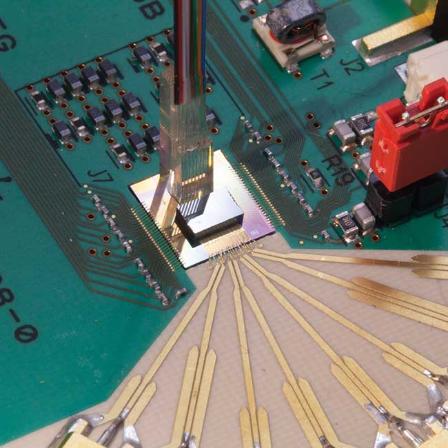
Figure 2. A 100-Gb/s receiver with a four-electrical-channel TIA stacked onto a four optical channel PIC.
Thanks to low parasitics and reduced signal path between ASICs and PICs, this approach is particularly suited for 56 GBd (and beyond) data rate applications.
To increase even further the module aggregated bandwidth, while keeping the form factor as small as possible, full 3D integration approaches will also be required in the future. A short-term approach is the integration of through-silicon vias (TSVs), which are vertical electrical connections passing completely through the silicon substrate of the PIC. By achieving higher interconnect densities than wire bonding, TSVs pave the way to the development of high-speed photonic interposers requiring high input/output counts. Such integration will be a key enabler for next-generation devices, addressing terabit-scale modules in data centers, as well as optical network-on-chip in many-core processor interconnect architectures for high-performance computing (Figure 3).
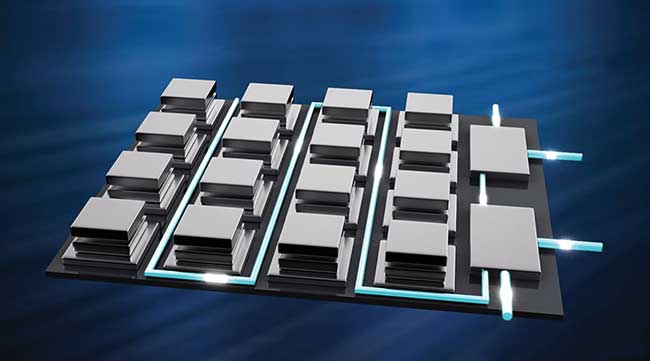
Figure 3. An example of high-speed optical network-on-chip interposer for many-core processor interconnect architectures.
Enhanced silicon photonics platform
Silicon photonics also offers the possibility of 3D photonic
circuitry using multiple layers of optical waveguides on the same chip.
With this method, at least two silicon photonic circuits could operate
together.
The different waveguide layers are placed close enough (i.e., 100 nm)
to deal with efficient optical coupling. This integration scheme offers
a new degree of freedom to designers, both to improve the performance
of existing components and to develop new photonic functions. An early
example of this approach pursued at Leti and STmicroelectronics within
European project H2020 COSMICC involves the introduction of a silicon
nitride optical layer, the refractive index of which is much less
sensitive to temperature than silicon (Figure 4). This property can be
exploited to build nearly thermally insensitive wavelength multiplexers
(MUX), which are required for low-cost coarse wavelength division
multiplexing (CWDM) datacenter applications where the PIC will remain uncooled. In such cases, thermally
insensitive MUX are required to cope with ±10-nm laser wavelength
variations for each channel. The silicon nitride layer can also be
advantageously used to achieve broadband input/output coupling to
optical fibers, also required for CWDM applications.
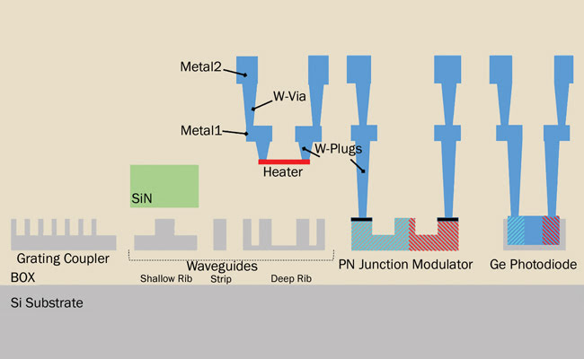
Figure 4. 3D photonic circuitry using two guiding layers made of silicon and silicon nitride.
Silicon photonics already offers a very attractive scalable platform to fulfill the demands of next-generation telecom and datacom interconnects. However, another key challenge is still the integration of laser sources. Until now, the laser source has remained separated from the rest of the chip, leading to high-cost packaging complexity and unavoidable coupling losses to the rest of the circuit. However, one promising short- and medium-term solution exists in the heterogeneous integration of III-V semiconductors with silicon through direct-bonding techniques. In this approach, unstructured InP wafers or dies are bonded with relaxed alignment tolerances, with epitaxial layers facing down, on a silicon-on-insulator wafer structured with optical waveguide circuits including passives, modulators, and photodetectors. After bonding, the InP growth substrate is removed and the III-V epitaxial film is processed. Leti has recently successfully developed a full 200-mm CMOS compatible process to fabricate PICs including hybrid III-V on Si lasers.
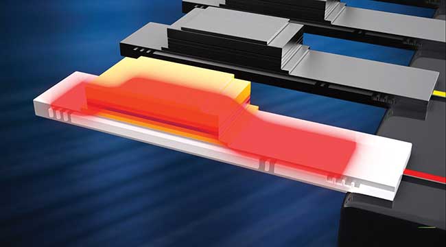
Figure 5. This illustration shows a laser source by heterogeneous integration of III-V gain medium on a PIC.
This approach exploits the highly efficient light-emission properties of III-V semiconductor materials, as well as the compact and low-loss photonic circuits on silicon. Light is generated in the III-V material and couples with the silicon circuitry thanks to the use of adiabatic tapers (Figure 5).
All the elements of the laser cavities — except the gain medium — are fabricated in the silicon, on which higher performance can be achieved thanks to the higher maturity of silicon fabrication processes, namely the cavity mirrors, such as Bragg mirrors, and additional filtering elements. Vertical fiber couplers are also fabricated in silicon for light output of the lasers.
A key achievement has been the integration of lasers on silicon for various communications applications. Tunable lasers over a wide wavelength range of 40 nm up to 90 nm, with a power level close to that of bulk InP lasers, have been developed by III-V Lab and Leti for metro and access networks using dense wavelength division multiplexing (DWDM). Direct modulation of these tunable lasers at 25 Gb/s over 50 km has been demonstrated for use in access networks, thanks to integrated chirp management structures. Various kinds of optimized distributed feedback lasers, which feature a robust single-mode behavior and reduced linewidth, also have been developed successfully for datacenter applications, where low cost per bit-per-second is key.
Such hybrid III-V-on-silicon integration also offers new options for modulation and detection. Other active devices such as electro-absorption modulators, photodiodes and light amplifiers can also be realized by engineering of the III-V heterostructure. III-V Lab and Leti have achieved a preliminary demonstration of a transmitter circuit including a distributed feedback laser, an electro-absorption modulator and a semiconductor optical amplifier with error-free transmission over 25 km at 25 Gb/s, using the same epitaxial stack. In this perspective, one of the attractive features of heterogeneous integration using dies is the wide choice of gain materials, allowing separate optimization of lasers, III-V electro-absorption modulators, and photodiodes to build high-performance, high-speed, and low-power consumption transmitter circuits. Beyond III-V materials, this heterogeneous integration technology opens the door to implementation of various materials on PICs in order to address new functions and application fields.
Public-private partnerships
Based on the maturity reached by silicon photonics technology, new application areas are targeted for optical communications and beyond. Next-generation technologies and applications are in development in R&D public-private partnership initiatives such as Japan’s PETRA, France’s IRT NANOELEC, Europe's Photonics21 Public-private partnership, and AIM Photonics in the U.S.
For optical interconnects, the short- and mid-term goals are focused on the datacenter applications with migration of the optical transceivers closer to the electronics, from front panel modules to mid-board optics. The ultimate integration level goes one step further by considering optical networking at the chip level with 3D integration of photonics and electronics for many core processor architectures. Beyond optical interconnect applications, new areas for exploration include sensors for IoT, lidar for autonomous cars, imagers for augmented reality, and biophotonics for health care.