Photonics HandbookFeatures
Silicon-Based Photonics Platform Enables On-Chip Imaging with High Throughput
Using silicon nitride wafers with CMOS compatibility allows a wide wavelength range to be useful in a variety of fluidics and fluorescence-based analyses.
POL VAN DORPE, NIELS VERELLEN, AND STIJN JOOKEN, IMEC
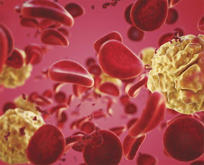
A close-up illustration of red and white blood
cells. Courtesy of iStock.com/matejmo.
Integrated photonics provides a framework for high-throughput applications, such as DNA sequencing, proteomics, and cell therapy, bringing a high level of parallelization and sensitivity to these domains. A CMOS-compatible silicon nitride (SiN) photonics platform that enables two new concepts in system design has been developed for such applications: an on-chip fluorescence microscope with a large field of view and high resolution, and an on-chip flow cytometer. The platform features advanced lithography and post-processing options as well as compatibility with fluidic packaging.
While systems exist to measure large arrays of fluorescent molecules in a short time, they are expensive and require long cycling times.
This technology has potential in the era of proteomics (the study of proteins). While systems exist to measure large arrays of fluorescent molecules in a short time, they are expensive and require long cycling times. The SiN platform, developed by imec, is characterized by a wide wavelength range (450 to 2400 nm) and low autofluorescence. Two iterations were created: an ultralow-loss SiN platform on 200-mm wafers, and a low-temperature option based on plasma-enhanced chemical vapor deposition, suited for post-CMOS processing. The latter can be integrated on both 200-mm and 300-mm wafers and with advanced 193-nm lithography options.
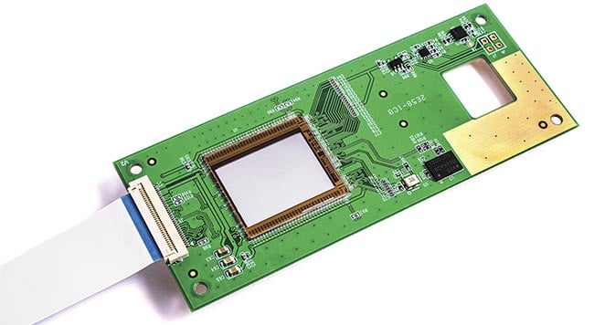
Figure 1. The silicon nitride (SiN) platform based on plasma-enhanced chemical vapor
deposition is a low-temperature option that allows post-processing photonics on top of
CMOS. Courtesy of imec.
Post-processing on top of CMOS or imagers has proved to be advantageous, when focusing on not only SiN photonics but also fluidics, microelectromechanical systems, and emerging materials, such as graphene and quantum dots, among others. It allows for a tight integration of different functionalities and thus compact and fast systems.
This article presents two recent advanced applications that use such a platform and illustrates the power of combining different functionalities, such as imagers and photonics, or fluidics and photonics1.
Subpixel microscopy
Based on the CMOS-compatible low-temperature SiN platform, an on-chip fluorescence microscope has been built with a large field of view and a high resolution. It is suited for parallel readout of large and dense molecular arrays like those used in proteomics.
The on-chip microscope consists of a pixel array or image sensor on top of which an SiN photonic circuit is processed. This circuit consists of waveguides and phase modulators. The waveguides guide the light toward the sample molecules, such as DNA/RNA molecules, peptides, and proteins, with attached fluorescent labels — in a microfluidic channel or in wells — while the phase modulators create tiny, structured illumination spots to precisely excite these fluorescent labels. A custom excitation filter (since it is part of a monolithic stack) is placed between the imager and photonic circuit to make sure that only the fluorescence emission, and not the excitation light, reaches the imager.
The structured illumination pattern is created by using constructive and destructive interference: A spot appears in regions in which the combined waves reinforce each other, while dark regions occur where the waves cancel each other out. A mathematical model was built to achieve a structured illumination pattern with a limited number of photonic components. This model was translated into an imaging chip architecture.
Because the integrated photonic circuit where the spots are generated is very close to the image sensor, the numerical aperture of the microscope is inherently high.
Currently, the key building blocks of the microscope are developed and validated, though the details are not yet published. The building blocks include the algorithms to design the structured illumination photonic circuits, the image reconstruction algorithms, the integrated optical phase modulators and beamsplitters, and the excitation filter. Also, the process flow for the deposition of active components, waveguides, and interference filters on imager wafers is set up. Further, proof-of-concept chips have been designed, fabricated, and packaged. They have been used in experiments to demonstrate and validate the on-chip optical lattice illumination and the lens-free high-resolution readout.
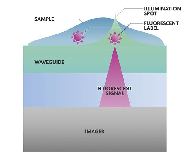
Figure 2. The on-chip fluorescence microscope consists of an imager with silicon nitride
(SiN) waveguides and phase modulators on top. Illumination spots are generated in the
photonic circuit to excite the fluorescent labels on the target molecules or cells. Next, the
imager picks up the signal. Because the photonic circuit is very close to the image sensor,
the numerical aperture of the microscope is high. Courtesy of imec.
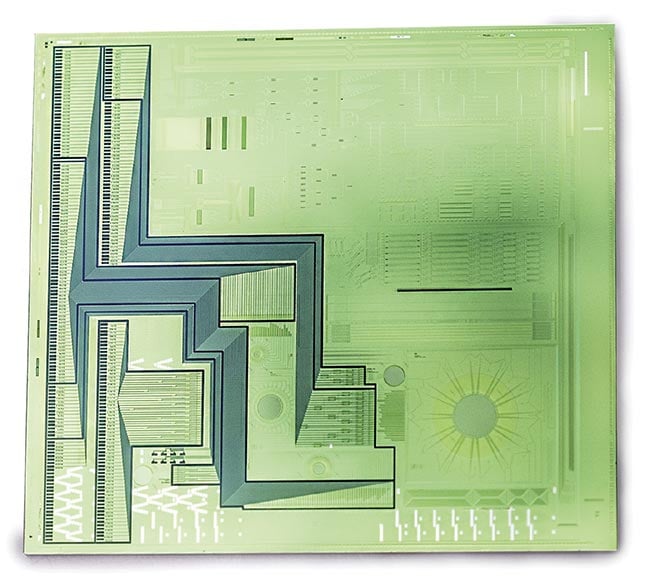
Figure 3. A proof-of-concept chip for subpixel lens-free fluorescence microscopy. More
specifically, the chip consists of a CMOS imager chip with monolithically integrated photonics
on top: a dedicated fluorescence filter and active photonic circuitry containing silicon
nitride (SiN) waveguides, electrical connections to optical modulators, and sensing areas.
Courtesy of imec.
The next focus in development will be scaling up to larger fields of view by designing several custom passive and active optical circuit components, including integrated optical phase modulators, integrated beam expanders, and combiners.
On-chip flow cytometry
A flow cytometer has also been fabricated with monolithically integrated photonics and fluidics, in a 200-mm CMOS pilot line. Technological advancements have made it possible to construct the chip by bonding three wafers, from bottom to top. The resulting layers contain illumination photonics, fluidics, and collection photonics. Compared with state-of-the-art flow cytometers, the integration of both excitation and collection photonics allows for an alignment-free device operation, drastically reducing instrument variability. Moreover, the co-integration of photonics with fluidics allows for parallelization of multiple channels, which increases the device throughput.
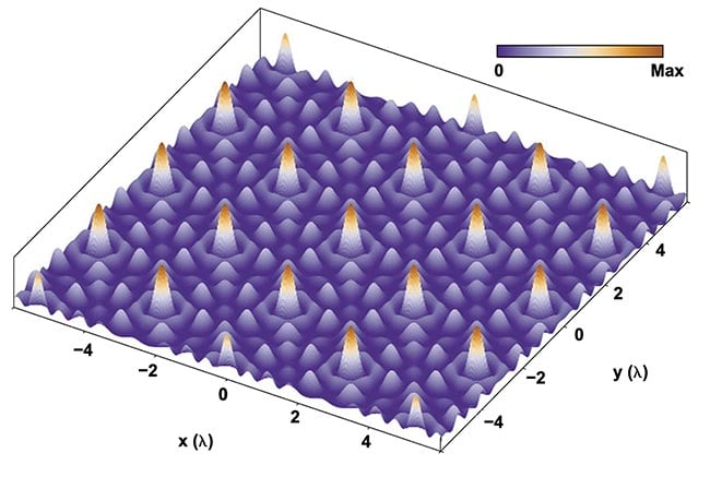
Figure 4. A mathematical model was built to achieve a structured illumination pattern, with
a limited number of photonic components. This model was translated into an imaging chip
architecture. The periodicity of the generated pattern is of the same order of magnitude as
the wavelength λ of the illumination light. The axes therefore denote integer values times λ.
Adapted with permission from Reference 2.
The key element of the illumination photonics layer is the illumination grating that directs the light upward through the fluidic channel. It is fabricated using the SiN photonics platform, characterized by low loss and low autofluorescence. The 638-nm light is coupled in the chip using a diffraction grating coupler and travels via a waveguide to the illumination grating.
The microfluidic channel consists of two channels for the sheath flow and one for the sample flow that are joined together to make up a well-aligned sample stream within a carrier/sheath fluid. At the optical interrogation points, cells or particles in the sample stream, for example, from a blood sample, are illuminated by the excitation light from the illumination photonics layer below. A waste outlet is located at the end of the microfluidic channel.
The collection photonics on top of the microfluidic channel are integrated in a quartz layer. There are gratings for the collection of forward scattered light and of side scattered light. The collected light is coupled in multimode waveguides, which transmit it to edge couplers and finally to fiber optics.
The performance of the on-chip cytometer was tested with a full peripheral blood mononuclear cell sample. These cells are produced in bone marrow. Both the forward and the side scattering from the illuminated cells could be reliably detected with the integrated collection photonics. It was possible to discriminate between monocytes, lymphocytes, and debris in a blood sample as well as with a benchmark flow cytometer3.
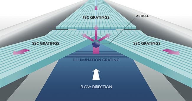
Figure 5. The on-chip flow cytometer consists of illumination photonics in the bottom
silicon layer, topped with microfluidics in silicon, and collection photonics in a quartz
layer. Light that is scattered in the forward direction is collected by forward scattered light
gratings, while the side scattering collection is collected by side scattered light gratings.
Adapted with permission from Reference 3.
The on-chip flow cytometer’s main advantage is its potential for parallelizing multiple flow channels, enhancing system throughput. Because it is CMOS-compatible, it can also be integrated with other functionalities such as a bubblejet sorter to create a GMP (good manufacturing practice)-compliant, closed-loop, multichannel device to identify and sort cells4. The technology is useful for all sorts of applications, such as cell therapy, in which imec collaborates with the Austrian deep tech startup Sarcura. The photonic components and layout are customizable: The number of interrogation points, the collection grating positions, and the illumination colors for fluorescent label excitation can be tailored to the specific application needs. Applications such as cell cycle analysis and proteomic profiling might require different excitation colors, depending on the fluorescent labels that are used.
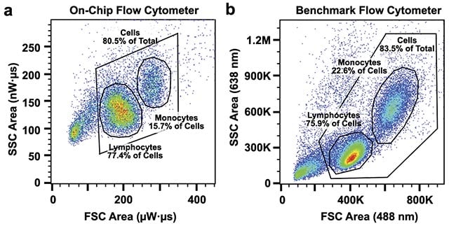
Figure 6. The monocyte and lymphocyte populations in a peripheral blood mononuclear
sample can be reliably discriminated on-chip (a) when compared to a benchmark flow
cytometer (b). FSC: forward scatter; SSC: side scatter. Adapted with permission from Reference
3.
A CMOS-compatible low- temperature SiN photonics platform is a key enabler for high-sensitivity and high throughput applications, such as fluorescence-based analysis in the field of proteomics, and cell identification and sorting in cell therapy manufacturing.
A CMOS-compatible low-temperature SiN photonics platform is a key enabler for high-sensitivity and high-throughput applications, such as fluorescence-based analysis in the field of proteomics, and cell identification and sorting in cell therapy manufacturing. Two innovations, the aforementioned on-chip fluorescence microscope and flow cytometer, have demonstrated the platform’s capabilities and versatility.
For both systems, the manufacturability of readily available components was considered from the start. They were processed in a 200-mm cleanroom, with state-of-the-art equipment and a well-thought process flow for integrating CMOS, photonics, and fluidics.
Meet the authors
Pol Van Dorpe started at imec as a summer intern in 1999 and later joined as a Ph.D. student in 2001. Since 2012, he has held a position as a part-time associate professor in the physics department of Katholieke Universiteit Leuven (KU Leuven). His main research focus is enabling novel applications in the life sciences field using integrated photonic concepts. His efforts were recognized as he earned the title of imec fellow in 2020; email: [email protected].
Niels Verellen is scientific director and R&D team leader of integrated biophotonics at imec’s life sciences technologies department. He develops integrated photonics solutions for life sciences applications and is a research fellow at the KU Leuven Quantum Solid-State Physics group. He received his master’s degree and Ph.D. in physics from KU Leuven. He was awarded the Umicore Scientific Award in 2012 and received a European Research Council (ERC) Starting Grant in 2018 to develop a high-resolution on-chip and lens-free fluorescence microscopy platform; email: [email protected].
Stijn Jooken is a biophotonics researcher at imec’s life sciences technologies department. He holds a master’s degree in applied physics from Eindhoven University of Technology (TU/e) and a Ph.D. in physics from KU Leuven. His work involves integrated photonics for life sciences applications with a focus on the development of silicon nitride (SiN)-based platforms for cell detection and fluorescence biosensing; email: [email protected].
Acknowledgment
The work on the on-chip fluorescence microscope is part of a project that received funding from the European Research Council (ERC) under the European Union’s Horizon 2020 research and innovation program (Grant Agreement No. 805222).
References
1. E. Parton et al. (2024). Monolithic microsystems. imec, white paper, www.imec-int.com/monolithic-microsystems.
2. S. Libbrecht et al. (2024). A microfluidics approach for ovarian cancer immune monitoring in an outpatient setting. Cells, Vol. 13, No. 1, p. 7.
3. S. Jooken et al. (2024). On-chip flow cytometer using integrated photonics for the detection of human leukocytes. Sci Rep, Vol. 14, No. 10921.
4. D. Kouznetsov et al. (2020). Revival and expansion of the theory of coherent lattices. Phys Rev Lett, Vol. 125, No. 18, p. 184101.
/Buyers_Guide/Imec/c22187
Published: September 2024
Glossary
- fluorescence
- Fluorescence is a type of luminescence, which is the emission of light by a substance that has absorbed light or other electromagnetic radiation. Specifically, fluorescence involves the absorption of light at one wavelength and the subsequent re-emission of light at a longer wavelength. The emitted light occurs almost instantaneously and ceases when the excitation light source is removed.
Key characteristics of fluorescence include:
Excitation and emission wavelengths: Fluorescent materials...
- integrated photonics
- Integrated photonics is a field of study and technology that involves the integration of optical components, such as lasers, modulators, detectors, and waveguides, on a single chip or substrate. The goal of integrated photonics is to miniaturize and consolidate optical elements in a manner similar to the integration of electronic components on a microchip in traditional integrated circuits.
Key aspects of integrated photonics include:
Miniaturization: Integrated photonics aims to...
- lithography
- Lithography is a key process used in microfabrication and semiconductor manufacturing to create intricate patterns on the surface of substrates, typically silicon wafers. It involves the transfer of a desired pattern onto a photosensitive material called a resist, which is coated onto the substrate. The resist is then selectively exposed to light or other radiation using a mask or reticle that contains the pattern of interest.
The lithography process can be broadly categorized into several...
- fluorescence microscopy
- Fluorescence microscopy is a specialized optical imaging technique used in biology, chemistry, and materials science to visualize and study specimens that exhibit fluorescence. Fluorescence is the phenomenon where a substance absorbs light at one wavelength and emits light at a longer wavelength. In fluorescence microscopy, fluorescent dyes or proteins are used to label specific structures or molecules within a sample.
The basic principles of fluorescence microscopy involve illuminating the...
- flow cytometry
- Flow cytometry is a powerful technique used in biology and medicine for the quantitative analysis of the physical and chemical characteristics of cells and particles suspended in a fluid. The method allows for the rapid measurement of multiple parameters simultaneously on a cell-by-cell basis. It is widely used in various fields, including immunology, microbiology, hematology, and cancer research.
Here are the key components and features of flow cytometry:
Sample preparation: Cells or...
Featuressiliconsilicon nitrideon-chipCMOSfluidicsfluorescenceintegrated photonicsplasma-enhanced chemical vapor depositionlithographyDNARNAblood cellsstructured illuminationactive componentsfluorescence microscopyflow cytometry