Transforming ordinary materials into extraordinary optics holds the key to progress.
Hubert Kostal, NanoOpto Corp.
Optics today needs alchemy, and the forces that motivate microchip technology are a key reason why. Today, light can transmit and process digital information as well as electricity can — in some ways, even better. But exploiting this potential requires the optical equivalent of microchips and the optical alchemy able to create them. However, what we have had to date is largely the outgrowth of a centuries-old technology: bulk optics.
Old optics, new applications
From the days of the early lens grinders, bulk optics manufacturers have focused on bringing real-world images to the human eye. As a result, traditional bulk optical elements — lenses, mirrors and filters — have been optimized to handle visible wavelengths for visual purposes and built on a scale appropriate to the view and the viewer.
Meanwhile, the digital domain has opened up new realms of optical applications neither coupled to the eye nor scaled to the familiar world. Currently, optics serves such applications as astronomy, microscopy, photography and visual correction while complementing and competing with electronics in information-processing applications such as imaging and projection, data storage, communications, industrial robotics, precision measurement and machining.
Limitations of the past
In many applications, bulk optical technology lacks the qualities that give microelectronics its vast applicability and world-changing power.
For example:
• Compared with microchips, whose density has doubled every 18 months throughout the past four decades, bulk optical elements are massive and do not gracefully scale down to an ideal size range.
• Compared with microelectronics — which derives endless versatility and applicability from a relatively unified core of materials, processes and design elements — bulk optical technology must expand its application range with a disparate collection of natural and manufactured materials because each material has relatively fixed optical properties and functions.
• The raw materials of bulk optical technology require widely varied manufacturing methods, limiting the economies of scale that so powerfully propel microelectronics.
• Whereas ever-growing integration is the essence of microelectronics, integration is difficult to achieve in bulk optics because its various materials and manufacturing methods are often incompatible.
As a result, microelectronics has become extremely pervasive. To keep up, photonics must match this breadth of application and ease of use.
Nano-optics to the rescue
Now a relatively new optical technology, nano-optics, is bringing photonics the optical alchemy it needs to complement microelectronics.
Nano-optics addresses every shortcoming of bulk optics mentioned above and shares the key strengths of microelectronics. Like microelectronics, and unlike bulk optics, it is a set of functional, integrated building blocks united by a common manufacturing method.
Nano-optics takes different forms and works on different principles than bulk optics. Nano-optic elements consist of numerous nanoscale structures created in regular patterns on or in a material. Depending on the optical function, operating wavelengths, and manufacturing requirements, they are created in a range of metals (e.g., gold or aluminum), dielectrics (e.g., silicon dioxide or silicon nitride), III-V materials (e.g., Si or GaAs), epitaxially grown crystals, glass and plastics. In whatever form, the act of creating the nanostructured material is transformative.
These structures often take the form of an ultrafine-scale diffraction grating with typical dimensions on the order of tens of nanometers to several hundred nanometers. This allows nano-optic devices to perform optical functions in very thin layers, often less than a micron in thickness. Because the subwavelength-size structures of nanopatterns interact with light locally, involving quantum effects as well as classical optical principles, they achieve their optical effects in an extremely short focal length compared with bulk optics. This allows for a very compact form factor sized for optical component architectural requirements.
Versatility and tunability
Nano-optics draws on a coherent design vocabulary functionally equivalent to the design libraries of semiconductor fabrication. These design options can be selected and combined to provide all the standard optical functions (polarization, phase, wavelength and propagation management) required for practical optical components, circuits and systems.
Design options include:
• varying the height, width and period of the grating
• creating two-dimensional or multidimensional gratings
• choosing various materials for the substrate and the grating
• employing a grating/fill material
• coating the grating/fill surface.
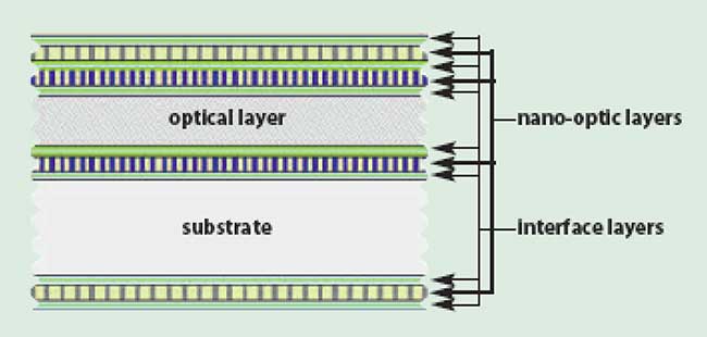
Variously deploying and combining these options not only provides the overall functionality desired, but also tunes and optimizes device functionality both optically and physically — affecting temperature tolerance, wavelengths of operation and acceptance angles, for example. The general construction of a nano-optic device is illustrated in Figure 1.

Figure 1. A generic nano-optic device is an optical system consisting of one or more nanostructure layers, thin-film interface layers, optically functional layers and a substrate, or core. This system allows optics ranging from simple discrete devices with a single nanostructure layer to complex, arrayed, electronically controllable optical components to be designed and fabricated.
Cost- and volume-efficiency
While the concept of nanoscale optical elements has been explored for some two decades, the manufacturing technologies necessary to commercialize the concept have only recently come online. Researchers have built subwavelength grating structures with costly, high-energy, low-volume techniques such as electron-beam lithography, or with techniques that have inherent limits in the range of structural patterns that can be achieved such as molecular self-assembly.
To achieve the requisite economies of scale, a manufacturing process more akin to semiconductor methods is needed. Nanopattern transfer satisfies this requirement through a combination of printing and semiconductor manufacturing operations. Because this nanolithography approach forms nanopatterned masks through a direct, physical process rather than with energy beams, pattern resolution is not compromised by wave diffraction, scattering and interference in the resist. This facilitates extremely small feature size and opens the way to further miniaturization as the technology evolves.
By re-using and replicating nanopattern masters, nano-optic production rates and volumes can be easily scaled to meet demand, and initial tooling costs are amortized over the multiple production runs for multiple products. And because nano-optics, like microelectronics, involves the wafer-based production of numerous compact devices on each substrate, high volumes are far easier to attain within a given time and cost than with bulk optical manufacturing processes that produce one optical element at a time.
Several factors make nano-optical elements ideal for integration into multielement devices.
• Nano-optics can often be closely coupled with other components in optical assemblies because of their compact optical interactions, thus making alignment in assembly more forgiving, less labor-intensive and less costly.
• They can be monolithically self-integrated by stacking nano-optic layers to create aggregate optical effects. Nanopattern transfer allows direct layering onto a single substrate without the complication and cost of multidevice lamination.
• Nano-optics can be spatially integrated by organizing varying optical functions into an array structure. This is achieved by creating a pixelated master and transferring the entire array structure in a single operation. These arrayed devices can be applied in multibeam or multipath optical circuits, eliminating the need to align discrete optics individually.
• Hybrid integration can be achieved by adding a nano-optic layer or layers to functional optical materials. The process by which nano-optic elements are fabricated is flexible and robust, allowing for cost-saving manufacturing process integration in creating hybrid optics.
• Integrating nano-optics with optically active layers can create optical control circuits — complex optical components on a chip. For example, multilayer nano-optic integration has been demonstrated by combining filters with photodetector arrays to create dynamic optical feedback loops.
Nano-optics can be used to make a variety of discrete optical devices with functions directly comparable to those of existing bulk optics (although often smaller and more robust). Taking advantage of the unique physics of nano-optics also allows the creation of optical devices with functionality that is not available with bulk optics.
One does the work of two
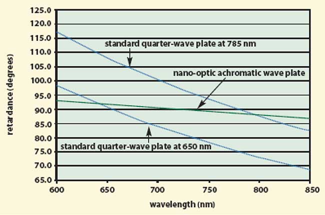
For example, nano-optics can be applied to create an achromatic, true zero-order, wideband wave plate — that is, a zero-order wave plate that provides uniform fractional wavelength (e.g., quarter wave) retardation across 150 nm of bandwidth (Figure 2). Such a device is used in optical circuits where wavelength-independent performance is required. The device improves upon existing multilayer, multimode technologies in virtually every significant measure, including size, robustness, uniformity and wavelength range.

Figure 2. By appropriate choice of nano-optic structure and materials, a nano-optic achromatic wave plate can be fabricated. Such a device uses only a single nanostructured layer to yield a true zero-order wave plate. For a nano-optic device designed for use in optical disc drive assemblies, this figure compares the retardance of the nano-optic device with standard wave plate performance.
Spanning a 630- to 800-nm wavelength range, for example, a nano-optic achromatic quarter-wave plate encompasses the 650 nm and 785 nm wavelengths used in CD/DVD combination drives. This enables one nano-optic device to serve in the place of two wavelength-specific conventional wave plates in two separate optical paths, providing more consistent performance while reducing parts. More importantly, it allows for optical circuit designs that combine the separate optical paths into a single path, creating a smaller, simpler optical circuit that requires less critical alignment in assembly, while delivering better and more stable performance at reduced overall cost.
Monolithically integrating multiple nano-optic functional layers into a single device can compound the advantages inherent in individual functional layers and create combinations of optical functionality that would ordinarily require the lamination of discrete bulk optic material layers.
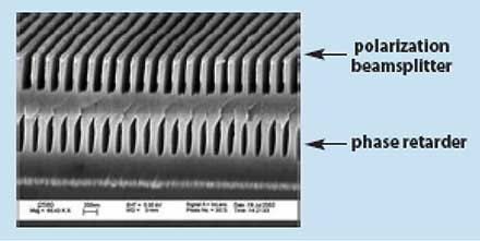
For example, an integrated nano-optic polarizer and wave plate fabricated on a single optical chip (Figure 3) can be used in a wide range of optical circuits. Combining this integrated device with photodetectors creates a high-speed optical feedback device for determining the polarization and phase state of incident light; such a device can be used for optical performance monitoring and sensor applications. Similar polarizer/retarder combinations can be applied to optical drive and projection display circuits, offering compelling cost, size and reliability advantages over the same functionality provided by individual bulk optic devices.

Figure 3. As shown in this scanning electron microscope photo, multilayer nanostructures have been demonstrated using nanopattern replication manufacturing techniques. This combination of a polarization beamsplitter and phase retarder is a subset of a nano-optic array designed as the core of an optical performance monitoring component.
Significantly thinner
A hybrid of nano-optics is a free-space variable optical attenuator (FSVOA) and shutter. This tunable optic addresses the frequent need to control and block the output power of polarized light sources, such as optical transceivers, in order to dynamically optimize their signals and to facilitate maintenance.
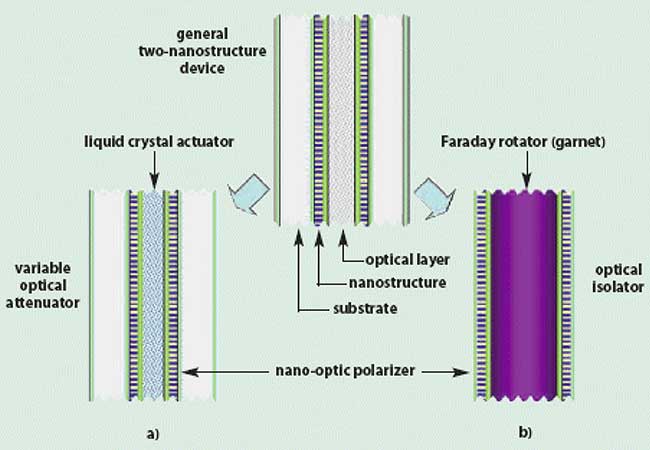
The nano-optic-enabled FSVOA consists of a crossed pair of polarizing nanostructures sandwiching a liquid crystal cell; applying an electrical field across the liquid crystal will rotate the liquid crystal molecules and control the fraction of light that passes through the structure (Figure 4a). Because the nano-optic polarizer is directly integrated into the liquid crystal cell construction, this allows the entire component to be less than 1 mm thick — three to 10 times thinner than conventional technologies — with the nano-optic contribution being less than 2 μm thick. In reliability and consistency, this FSVOA can be expected to compete favorably with mechanical VOAs because nano-optic structures are inherently robust, LCD technology has no moving parts, and this device provides accurate, stable, repeatable attenuation over temperature without closed-loop feedback via direct AC voltage control or optional I2C control. This nano-optic-based design concept has been used to create other tunable devices, including tunable spectral filters.

Figure 4. As shown in this scanning electron microscope photo, multilayer
nanostructures have been demonstrated using nanopattern replication
manufacturing techniques. Sandwiching a liquid crystal actuator layer between two nano-optic polarizers yields a variable optical attenuator and shutter. Constructing a nano-optic polarizer on either side of a Faraday rotator yields an optical isolator. Applications exist for both telecom transceivers and nontelecom optical circuits.
Hybrid integration of nano-optics can radically simplify components as well as shrink them, as a nano-optic-based optical isolator illustrates. An optical isolator prevents the light from optical communications networks from scattering back into the lasers and degrading their output power and wavelength stability. It provides the same functionality as conventional optical isolators, allowing only one-way light transmission, in a form with compelling physical and fiscal advantages.
Conventional isolators consist of multiple polarizers and Faraday rotators, laminated or air-spaced together in a magnetic field. Their polarizing component alone can measure up to 0.5 mm thick. By contrast, the nano-optic isolator employs submicron-thick polarizing nanostructures fabricated directly on the garnet surface of a Faraday rotor (Figure 4b). The resulting assembly is less than half the thickness of conventional isolators, while eliminating the refractive penalties of epoxy from the beam path. This compactness and simplicity streamlines manufacturing and facilitates a smaller, lower cost, higher performance transceiver package.
If we accept microelectronics as a model of practical alchemy, we have reason to believe that nano-optics may have a similar, sweeping impact.
Microelectronics has transformed the world not through a one-step, lead-into-gold transmutation, but rather through a spiraling interaction of simultaneous and ceaseless advances in device miniaturization, density, integration levels, capability and cost/performance. The stage is set for nano-optics to spread and ascend along the same lines.