Operating in the nano-realm offers designers a host of new opportunities. Understanding what to expect in this miniature world is key to successful nano-optic component design.
Hubert Kostal, NanoOpto Corp.
When physical structures get very small — on the order of molecular or atomic sizes with one or more dimensions on the nanoscale — their behavior and interactions with energy, including light, differ greatly from those of larger, macroscale structures. This is important for optical circuits for two reasons. First, the different physical behavior provides the optical component designer an entirely new realm of optical functions. Second, changing dimensions, shapes, spacing and materials provides almost infinite flexibility in the variation of optical functions because the realized optical properties are modulated by the nanoscale physical structures.
Today, optical component and circuit designers find themselves simultaneously needing to meet requirements for delivering increased performance and functionality, while continually reducing costs and size. Bulk-optic-based optical circuits, while benefiting from years of accumulated efficiency gains, face significant technology barriers to achieving the cost and integration levels that are required for next-generation optical systems for consumer electronics (e.g., optical data storage, digital imaging and display), industrial optics (e.g., sensors and control systems), and optical communications (e.g., transceivers and optical routing) applications.
A difficulty in designing cost-effective optical components and circuits is the gap between today’s optical devices and their semiconductor counterparts in the dimensions of integration, density, diversity, manufacturability, availability and reliability. There are several key reasons for this gap. First, for the most part, different optical functions often can only be achieved by using different physical materials. This in turn requires multiple, discrete manufacturing technologies which limits production efficiency, the depth of integration that can be realized, and drives up individual device costs. Aggravating matters, the natural optical properties of many discrete optical elements are relatively fixed, limiting options for the optical component designer and reducing design transferability — a stark contrast to the high flexibility and reusability of semiconductor design elements.
Nanostructure-based optical components — “nano-optics” — address these cost issues by taking integrated optical component design to the next level of density, cost and reliability. By manipulating the size, shape and period of the nanostructures in the optical beam path, nano-optic components deliver a broad range of useful optical effects, creating an enhanced set of optical element building blocks. These discrete building blocks have individually excellent optical properties and easily integrate with other optical materials in a broad range of configurations. In addition, nano-optic building blocks self-integrate to allow increased flexibility in optical component design while reducing part counts and increasing reliability in optical components and systems.
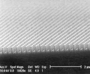
Figure 1. SEM photo of the cross section of a nano-optic grating structure.
Nanostructures
Nano-optic components are based on nanoscale structures arranged in periodic patterns on an optical substrate with critical dimensions much smaller than the wavelength of the light that passes through them. For applications at the IR, visible and UV wavelengths, the useful dimensions of these structures range from several hundred to less than 10 nm. To achieve their intended optical effects, the nanostructure need be only a fraction of a wavelength thick. By contrast, bulk optical elements typically involve structures many times larger than the wavelengths of light, both to provide the desired optical behavior and to facilitate manufacturability. A scanning electron microscope (SEM) view of a cross section of a typical one-dimensional subwavelength grating structure is shown in Figure 1.
Nano-optics can also be created with nanostructures in one, two or three dimensions. Depending on the configuration of the nanostructures and the constituent materials used in their construction, these devices can function as:
• polarizers
• polarization beamsplitters and combiners
• wave plates
• filters
• microlenses
• antireflective and diffusive coatings
and more. The precise physical behavior of nano-optic structures can be modeled by rigorous application of diffraction grating theory and the boundary conditions of Maxwell’s equations. Different behavior with respect to reflection, refraction, diffraction and interference occur when compared with traditional, bulk optical structures.
In general, the interaction of light with a nanostructure results in both a transmitted and a reflected component, as shown in Figure 2. There are four general classes of nano-optic properties, based on the property of light that they affect: polarization, phase, wavelength, and propagation.
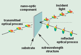
Figure 2. The interaction of a nano-optic component with an incident beam of light results in both a transmitted and a reflected function.
A polarization management nano-optic device transmits one polarization and reflects the orthogonal polarization. By adjusting structural parameters and antireflection coatings, the insertion losses for the transmitted and reflected components, as well as their extinction ratios, can be controlled to meet various application requirements. The thickness of the active layer of the subwavelength grating required is less than 1 μm. These properties result in some unique benefits of nano-optics polarization beamsplitters/combiners (PBS/C). First, because the structure size is far smaller than the wavelength of light, form factors can be extremely small — close to the size of the incident beam. Second, because the nanostructure is nonabsorptive, the PBS/C has a high power handling capability. Third, subwavelength gratings exhibit only zero-order diffraction effects, with no higher order diffraction, resulting in both uniform optical performance over a broad wavelength range — for example, the same physical grating structure behaves as a PBS/C for 980 to 1800 nm wavelengths — and a wide acceptance angle — plus or minus 20° about normal incidence. Similar effects hold over other wavelength ranges as well.
Similarly, adjusting the nanostructure dimensions can create phase management functions such as phase retardation and wave plates. By proper choice of dimensions, zero-order wave plates with wave retardation down to 1/100th of a wavelength with excellent lateral uniformity are realized. Wavelength management functions — narrowband and broadband optical filters, both polarization dependent and polarization independent — can also be created with application-specific passband shapes. Propagation management nano-optic devices can control the focal properties of light, yielding antireflective coatings, diffusive structures, lens arrays and blazed gratings. By incorporating an electrical or magnetic actuator, tunable nano-optic devices can be built.
Optical integration
Subwavelength optical elements provide a new set of building blocks for integrating optical functions. Two approaches to integration are possible: hybrid and monolithic. Hybrid integration takes dissimilar technologies and combines them into optical components; monolithic integration self-combines nano-optic elements into more complex, layered optical components.
Discrete nano-optic devices add breadth to the toolkit of the hybrid integrated optical circuit designer, creating multiple advantages. Individual nano-optic devices often provide density, optical power handling, optical coupling, and compatibility advantages over the bulk optic counterparts. Appropriate selection of materials provides uniform performance over a broad range of optical power and environmental requirements. In addition, material selection or direct integration with other technologies can simplify cross-technology interfaces. By providing a broad range of fundamental building blocks for optical component and module design, nano-optic components enable both new functions and new combinations of functions.
Nano-optic components also offer advantages for manufacturing hybrid integrated optical components. The wide acceptance angle of many of these devices simplifies the alignment process, reducing manufacturing time and cost. Additionally, the robustness of nano-optic devices — with proper selection of materials they can be subjected to temperature ranges of –200 to 400 °C — makes them tolerant of a broad range of manufacturing operations.
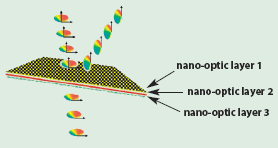
Figure 3. Nano-optics can be monolithically integrated by combining both pixel arrays and by layering to create complex optical functions.
Monolithic integration of nano-optic devices is achieved by a manufacturing process that can simultaneously create pixel arrays and stacks of nano-optic structures, thereby creating aggregated optical effects (Figure 3). This technique can combine adjacent optical devices into a single device; for instance, merging a polarizer and a wave plate on a single optical chip. Adding optically active layers allows optical control circuits to be built, resulting in complex optical components “on a chip.” For example, a polarizer/wave plate nanostructure together with photodetectors can be combined to provide a high-speed feedback device for determining the polarization and phase state of the incident light.
Nanopattern transfer
Despite their promise and novel benefits, up until a few years ago nano-optic devices have been studied primarily through theory and simulation because of the difficulty and high cost of their fabrication. To suit these devices to high-volume, low-cost commercial applications, the challenge has been to develop a fabrication technology that approaches the efficiency of semiconductor fabrication.
Generally speaking, nanoscale structures can be created by a number of methods — electron-beam lithography, holographic lithography techniques, self-aligned structure growth, and others. Each of these approaches has practical limits for commercial application, including cost, complexity, yield, volume, and limited application to the production of diverse structures. Nanopattern transfer is a wafer-scale nanolithography fabrication methodology that overcomes these limits. The process involves four key steps: selecting a master plate inscribed with the complement of the desired nanopattern, contacting this master with a resist-coated wafer to transfer the pattern to the resist, selectively removing the resist with reactive ion etching (RIE) to transfer the nanopattern to the target material; and postprocessing to add protective and functional thin film layers over the nanostructure. This process is shown in Figure 4. Because nanopattern transfer creates the nanostructure etching mask by a direct, physical process rather than by beams of energy, the effects of wave diffraction, scattering and interference in the resist do not limit fabrication resolution.
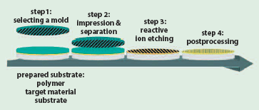
Figure 4. Nanopatterning is a highly repeatable, wafer-scale process for creating nano-optic components.
Once processed, the wafer is mapped via optical and visual testing, and then diced to yield optical chips such as those shown in Figure 5. The size of the nano-optic device used in an optical application may be as small as 1 mm × 1 mm on a substrate of a thickness of 0.1 mm to tens of millimeters square on a thicker substrate.
The master used to imprint the subwavelength structures, an essential ingredient in the process, can be created using various techniques, including holographic and electron-beam lithography. Because the mold can be replicated and reused, complex multistep and multiprocess methods can be used to create complex nanostructure patterns. Since these initial tooling steps do not need to be repeated for each production wafer, the investment is amortized over the complete production run of a particular nano-optic device. Using different masters with different nanostructure patterns allows the same manufacturing process to create the full range of optical components.

Figure 5. Nanopatterned wafers are diced into nano-optic chips for application in optical systems.
As a wafer-scale manufacturing technology, the nanopatterning process shares many positive attributes with semiconductor manufacturing. It easily scales by increasing wafer runs, or by replicating manufacturing lines. Different devices are produced on the same manufacturing line by selecting the appropriate mold and adjusting process parameters. It can be run as a single-step or multistep process, creating simple, single-layer devices or complex, multilayer devices.
Conclusion
Because nanopatterning is a highly scalable, automated process for the fabrication of nano-optic components, they can be manufactured at high volumes and low costs generally unapproachable in the world of bulk optics. The variety of optical functions and ease of integration that can be realized with nano-optics change the rules for designing integrated optical components.
Currently available nano-optic devices — including polarizers, polarization beamsplitters and combiners, wave plates and filters — have immediate application to hybrid integration. As additional nano-optic building block functionality becomes available, engineers and designers will enjoy additional flexibility in integrating optical components, both hybrid and monolithic.