The EPIC Technology Meeting on Laser Microprocessing demonstrated the maturity of technological building blocks for microprocessing with ultrashort-pulse lasers.
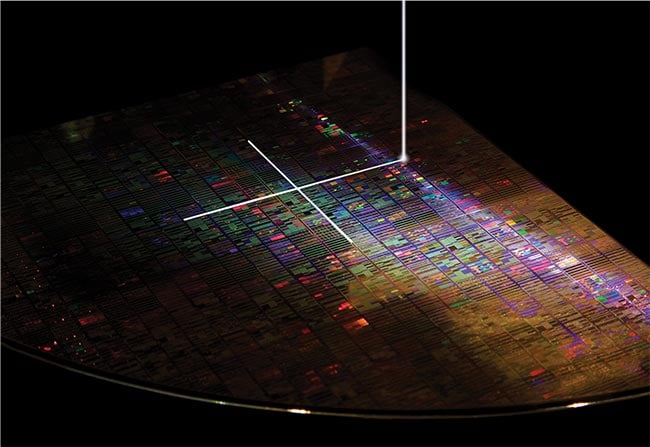
Courtesy of Amplitude Laser.
Laser microprocessing has been on the rise for decades. While technological roadblocks have influenced this progression, a close look at these roadblocks reveals that each has advanced to maturity. Productivity is key, and laser sources, scanners, and systems technology have made extensive progress; they are already used in large-scale applications, and much more growth is expected.
Laser sources and scanners
In the 1990s, scientists found that laser pulses in the pico- and femtosecond regime could be used to cut and drill almost any material with significantly reduced heat-affected zones and smoother walls compared with nanosecond pulses. Evidently, these ultrashort pulses (USPs) were well suited for drilling submillimeter holes and/or micro-structuring surfaces.
During the following 20 years, application research refined this scientific result and defined a process window for USP laser processing (i.e., which pulse energies provided the highest ablation efficiency). The researchers found that for efficient processing, the pulse energy (in fact, it is the intensity) cannot be scaled to infinity. Simplified, the pulse duration should be below a picosecond, with pulse energies in the tens of microjoules range for small spots. Repetition rates can be set up to megahertz or even gigahertz, and pulse trains can improve the effectiveness of these pulses.
As some scientists would say, “The rest is just engineering.” But it was not that easy. It took substantial inventions and countless feats of engineering to transform USP lasers from fragile lab instruments into rugged systems in OEM enclosures suitable for around-the-clock manufacturing processes.
These workhorses have been in the field for about a decade, running 24/7 without degradation in performance. At the European Photonics Industry Consortium (EPIC) Meeting on Laser Microprocessing in Vilnius, Lithuania, (read more here), Martynas Barkauskas, CEO of Light Conversion, demonstrated how reliable today’s sources have become when he shared performance data from some of the systems that Light Conversion has tracked in the field. These systems have essentially remained constant during 14 years of continuous operation. The company specifies more than 3 years’ mean time between failures for its systems.
With uptime no longer posing a problem, source manufacturers explored several ways toward achieving increased productivity from their systems. One method is to look for higher repetition rates, improving systems toward megahertz or gigahertz rates. Scanners were not designed for such speeds and have become a bottleneck. These source manufacturers also have looked to short bursts to increase the throughput: In response, several have developed burst mode controls and looked for higher pulse energy. While physics limits the reasonable intensity to ~7× the ablation threshold, a higher pulse energy can be exploited for parallel processing with multibeam optics or processes with tailor-made beam shapes, such as Bessel beams.
All of these developments are ready for industrial production. For example, pulse triggering for bursts and varying pulse distances for curved shapes were already reported in 20231. Improvements with scanners and multibeam optics are also underway.
Numbers for context
Now, how do these developments contribute to throughput? Consider the values presented by Mantvydas Jasinskas, chief science officer of EKSPLA. In application tests on aluminum oxide ceramics, he demonstrated that EKSPLA ablated 6.4 mm3/min with single pulses. With a single 92-pulse gigahertz burst, the scientists moved 10.4 mm3/min. And with a megahertz sequence of single pulses, they still achieved 5.2 mm3/min and 52.1 mm3/min with a gigahertz burst in megahertz sequences.
This rate further increases with back-side ablation, in which the laser shines through glass and its focus moves upward. For this bottom-up milling approach, Jasinskas showed ablation rates of 619.5 mm3/min (using a 2-MHz laser with 24-GHz bursts) in a soda-lime glass.
What about more power? Vincent Rouffiange, vice president, strategic business development director at Amplitude Laser, showed the evolution of the company’s lasers to 1 kW and beyond. With each more powerful source, he said, people thought no one would ever need such lasers. But the experience that Amplitude found in the market is different. As a result, the company has increased the source power during the last several years. Time and cost arguments are behind this decision. Rouffiange estimated that processing time (T) relates to the source power P by T ~ 1/P2.
All of this is to say that, apparently, source power does matter. Rouffiange expects that a 1-kW USP laser will arrive below €1000 per Watt. Considering the participants of the EPIC workshop and market research, it seems that regular USP laser sources with output powers between 10 and 300 W are standard off-the-shelf products. A few companies offer sources with ~1-kW output power, but these are either marketed as prototypes or sell in low numbers.
Aside from higher power, laser source providers are expanding to other wavelengths, such as UV (343 nm) or deep-UV (257 nm). These systems are available with reasonable lifetimes. Light Conversion, for example, specifies a 50-W UV source with a lifetime of 10,000 h or one year. Scanner solutions for these wavelengths were discussed at the EPIC workshop. It does not seem trivial today to change a complete scanner solution to accommodate UV optics.
Scanners keep pace
Ablation with USP lasers is still measured in cubic millimeters per minute. For obvious reasons, it is paramount to increase the productivity of USP laser-based microprocessing. As the optimization of laser sources has been a prime area of focus, scanning technology is the logical subsequent roadblock to obtaining more throughput. Scanners must move faster for lasers with higher repetition rates. Otherwise, pulses will overlap, which would not necessarily increase throughput.
Amplitude’s Rouffiange said that galvanometer scanners are now available with scanning speeds of up to 30 m/s, whereas a polygon scan head can reach up to 1000 m/s. In combination, both systems can serve in an industrial roll-to-roll solution with up to several meters per second throughput.
Selecting the appropriate scanner technology heavily depends on the applied process parameters — namely, repetition rate, pulse energy, and spot size. Each of these parameters depends on the application, Rouffiange said (Figure 1).
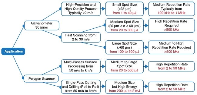
Figure 1. Combining advanced beam
steering and an ultrafast laser. Choosing the
right scanning technology depends on the
process parameters and ultimately the
application. Courtesy of Amplitude Laser.
On the other hand, scanners can be adapted to new wavelengths, as required for the respective beam sources. This adaptation can be far from trivial, according to Holger Schlüter, head of business development at SCANLAB GmbH. First, USP lasers require the use of fused silica as an optical material. Fused silica experiences a strong change of index (dn/dλ) in the UV, which makes color correction of the f-theta lens for wide-bandwidth pulses difficult. SCANLAB, for example, succeeded with an optimized lens design and a high-performance UV coating for this purpose.
Special optics make special beams
In the early days of materials processing, technology pioneers took laser sources with a defined beam profile and determined the tasks that they could accomplish. Today, this has changed completely: The application requirements define how the laser beam should look to realize the highest throughput. This is as true for laser macroprocessing as it is for microprocessing. And it is especially true for the shape of the beam profile. Fortunately, laser beams can be transformed into almost every shape (as Persephone Poulton, product development engineer from PowerPhotonic, showed (Figure 2)).
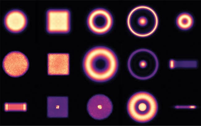
Figure 2. Modern optics can create almost
every beam profile needed, in almost any shape
and configuration. Courtesy of PowerPhotonic Ltd.
Behind such nice beam profiles is the consideration that a laser beam is a spatially distributed electromagnetic wave. Careful manipulation of the spatial and temporal phase of the laser beam leads to such profiles and to many more effects. A lens functions as a simple beam shaper, and more sophisticated beam shapers may use a micro-optical lens array to, for example, turn a Gaussian beam profile into a thin horizontal line expanding over 1 m.
Even more advanced systems, such as the one presented in Vilnius by Gwenn Pallier, product line manager at Cailabs, use reflective optics to create a Bessel beam, a very specific 3D beam profile with an extended focal length. While all of these optics are fixed, Lars Eng, CEO of Silicon Light Machines, presented a dynamic solution for phase manipulation. Silicon Light Machine’s solution uses a microelectromechanical systems (MEMS) chip for spatial light modulation.
Upscaling in process
Spatial phase modulation can be taken much further. It can turn one beam into a beam profile composed of many similar beams. This is a game-changing advancement because these beams can be used in parallel.
The multibeam optics concept was developed at the Fraunhofer Institute for Laser Technology ILT (Fraunhofer ILT) and commercialized by its spinoff Pulsar Photonics. The company applies the
multibeam optics in conjunction with multi-scanner or multi-gantry systems (Figure 3). Pulsar Photonics was acquired by the materials and machinery expert Schunk Group in 2022, and now has more than 100 employees. Pulsar, a systems integrator, focuses on upscaling laser processes regarding processing time and area.
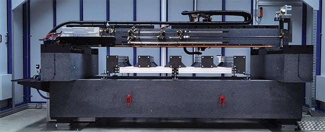
Figure 3. Pulsar Photonics combined multibeam
technology with a multi-gantry system and
offers industrial machines that are capable of
processing large volumes >10,000 cubic mm. Courtesy of Pulsar Photonics.
Multibeam optics can come in different shapes: Liquid crystal modulators or MEMS, for example, enable dynamic beam shaping, and diffractive optical elements (DOEs) achieve this in a static way. DOEs change the phase of the incoming beam by turning one beam into an array of hundreds, for example. In 2019, the Fraunhofer ILT researchers demonstrated a solution to drill 12,000 holes/s at micrometer precision using such beam-shaping optics.
Tim Kunze, CEO and cofounder of Fusion Bionic, showed a method for upscaling that goes deeper into application: Fusion Bionic’s machine uses interference fringes for texturing surfaces. This allows for pulse energies into the millijoule regime. Direct laser interference patterning is the company’s core technology, and it is well suited for making periodic patterns on extended square meter surface areas for the creation of so-called functionalized surfaces. Kunze also showed the solution for surface cleaning, though there may be a cheaper solution for this use case.
Lidrotec is pioneering an exotic and promising process. The company’s director of business development and sales, Christian Keil, introduced EPIC’s Vilnius audience to the company’s laser system that is designed to dice semiconductor wafers — a technology that brings the company into a huge and growing market. The solution performs the dicing through a thin layer of a nontoxic, transparent, low-viscosity liquid. Keil did not identify this fluid, but it is evident that such a solution could solve several problems currently associated with wafer dicing, including micro-cracks, debris, burrs, and more. Keil confirmed the company’s use of USP lasers. A pilot is running on Lidrotec’s premises, with a first machine delivery to a pilot customer planned for this year.
Where is the beef?
The proof of the pudding is in the eating. And similarly, the proof of the innovative technology that is behind this upscaling is in the application. This is not obvious and simple for USP laser microprocessing. The supply chain in this field usually consists of various component providers, systems integrators, and some big players — all of which tend to walk their own way.
In Vilnius, laser makers such as Amplitude, Light Conversion, EKSPLA, and ams Technologies (distinguished from ams OSRAM) showed that they are ready to serve any application needs. These companies can provide plenty of application examples. They include aluminum sorting based on laser-induced breakdown spectroscopy (neoLASE/ams Technologies); through-glass-via drilling (Fluence); marking and welding of aluminum (PowerPhotonic); dielectric material milling and drilling (EKSLPA); stent cutting, polishing, and periodic surface structuring (Light Conversion); and surface texturing and electrical vehicle electrode cutting (Amplitude, Light Conversion, among others).
This list is an ad hoc collection of samples; it neither aspires to name all applications, nor can it mention all providers of the respective technology. Many of the companies participate in collaborative projects to strengthen the technology, which Rouffiange showed.
The systems integrators are a bit more specific in their application reports. Etienne Pelletier, laser applications engineer at Oxford Lasers Ltd., spoke about laser micro-welding of transparent and opaque materials, such as glass and metal. 3D-Micromac was certainly one of the larger systems integrators in the room in Vilnius, with more than 600 machine installations worldwide, and Pelletier listed a range of applications that it serves. Currently, 3D-Micromac, he said, has more than 50 systems deployed in the semiconductor industry: at least 30 systems in micro-diagnostics, more than 110 systems in photovoltaics, and more than 30 systems in roll-to-roll production.
3D-Micromac has an additional 150-plus systems in glass and display — and its department head for technology and innovation services, Thomas Gester, gave an introduction into laser glass processing. This can be performed on the top of the material, from the bottom, or in the bulk material. The examples referred to sophisticated microprocessing tasks rather than those for consumer products.
Martin Reininghaus, program manager at Pulsar Photonics, then reported on applications in tooling, embossing, and the semiconductor industry. Pulsar’s latest machines process work pieces of 1 sq m with processing volumes beyond 10,000 cubic mm (Figure 3).
And then there was Andreas Russ from Bosch Manufacturing Solutions (BMG), a 100% subsidiary of the Bosch group. BMG is a turnkey special machinery provider for production equipment and automation. The company serves large industries such as automotive, energy, and consumer goods.
With a workforce of 1900 (including 42 laser experts) in nine locations, BMG has more than 4000 assembly and testing systems in the field. BMG’s laser activities focus on welding, structuring, drilling, cleaning, marking, and fine cutting (Figure 4). Projects that have reached milestones with USP lasers have involved precision drilling in diesel and gasoline injection systems. For gasoline direct injection systems, the machines have tolerances of a few micrometers and produce more than 250 million holes per year. The machines are highly automated with high-quality requirements and 100% traceability. They offer fully automated laser monitoring as well as an automated calibration portfolio.
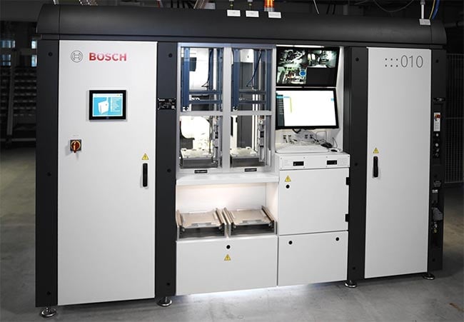
Figure 4. Bosch Manufacturing Solutions
(BMG) develops machines, including for
multistage hybrid laser microprocessing of
microelectromechanical systems (MEMS). The company’s activities focus on
laser welding, structuring, drilling, cleaning,
marking, and fine cutting. Courtesy of Robert Bosch Manufacturing Solutions GmbH.
In addition to this well-known automotive application, Russ discussed projects from the semiconductor industry. Bosch Manufacturing tested a two-laser multistep ablation system for silicon wafers. The effective ablation rate was >0.5 mm³/s, reaching a surface roughness of <0.5 µm.
In summary
It is safe to say that most aspects of the technology for laser microprocessing are mature. Currently, interesting ideas are entering the market at a beneficial pace, and certain ideas offer scaling opportunities for higher throughputs and extended workpiece areas.
As for what is on the way, applications such as precision tool making and semiconductor or glass processing are coming. The rapid growth of several players gives rise to the assumption that this field is prospering and that there is more to expect.
Reference
1. A. Thoss. (2023). Ultrashort-Pulsed Lasers Ramp Up the Power. Photonics Spectra, Vol. 57, No. 9, pp. 62-68.