Search
Menu
Edmund Optics - Manufacturing Services 8/24 LB
Photonics HandbookIndustry News

Metalenz, UMC Team for Metasurface Optics Market Launch

Facebook X LinkedIn Email
Metalenz has partnered with semiconductor foundry United Microelectronics Corp. (UMC) to begin mass production of its metasurface optics using semiconductor manufacturing processes. With this partnership, Metalenz said, metasurface optics will be available on the open market for the first time.

Rob Devlin, Metalenz co-founder and CEO, said that company is engaged in talks with OEMS to begin deploying metasurface optics in 3D sensing applications. Partnering with UMC, he said, grants manufacturing capabilities and a global reach to serve customers around the world.
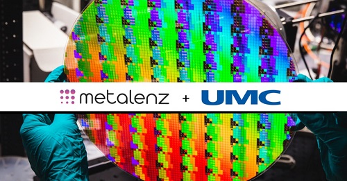
Metalenz has partnered with UMC to bring metasurface to the commercial market. Courtesy of Metalenz.
The first designs to go through the newly established supply chain will be for Chinese OEM DiluSense, a supplier of 3D sensing systems for IoT devices and consumer electronics. DiluSense founder and CEO Hu Lei said the integration of metasurface optics will enable new optical form factors and performance to further their 3D sensing AI solutions.

Metalenz’s technology has appeared in devices made in collaboration with STMicroelectronics. The company is a spinout of Harvard University founded in 2016.
Spectrogon US - Optical Filters 2024 MR


Published: June 2023
Glossary
metalens
A metalens, short for "metasurface lens," is a type of optical lens that uses nanostructured materials to manipulate light at a subwavelength scale. Unlike traditional lenses made of glass or other transparent materials, metalenses do not rely on the curvature of their surface to refract or focus light. Instead, they use carefully engineered patterns of nanostructures, such as nanoscale antennas or dielectric structures, to control the phase and amplitude of light across the lens's surface....
semiconductor
A semiconductor is a type of material that has electrical conductivity between that of a conductor and an insulator. In other words, semiconductors have properties that are intermediate between metals (good conductors of electricity) and insulators (poor conductors of electricity). The conductivity of a semiconductor can be controlled and modified by factors such as temperature, impurities, or an applied electric field. The most common semiconductors are crystalline solids, and they are...
time of flight
(TOF) The length of time needed for a signal to arrive at and be reflected from the target. The basis of an active autoranging/autofocus system.
lidar
Lidar, short for light detection and ranging, is a remote sensing technology that uses laser light to measure distances and generate precise, three-dimensional information about the shape and characteristics of objects and surfaces. Lidar systems typically consist of a laser scanner, a GPS receiver, and an inertial measurement unit (IMU), all integrated into a single system. Here is how lidar works: Laser emission: A laser emits laser pulses, often in the form of rapid and repetitive laser...
BusinesspartnershipcollaborationmetasurfaceOpticsmetalensmeta opticMetalenzUnited Microelectronics CorporationUMCsemiconductorfabricationsupply chain3D sensingtime of flightTOFlidarHarvardCapassoAmericasIndustry News

We use cookies to improve user experience and analyze our website traffic as stated in our Privacy Policy. By using this website, you agree to the use of cookies unless you have disabled them.