GABRIE HOOGLAND, PETER JOHNSON, AND VAMSY GODTHI, SABIC
With the combination of artificial intelligence, 5G networking, and high-performance compute necessitating dependable any-time connectivity, manufacturers of printed circuit board (PCBs) are searching for ways to enable higher bandwidth capacity and faster data transfer speeds. Traditional elements such as copper traces and flyover cable(s) face performance limitations and size constraints that generate high energy demands and costs. Optical components, including lenses and fiber arrays used in transceivers and connectors can surpass copper-based PCB designs in bandwidth capacity. These components also enable the use of co-packaged or onboard optics that can help increase bandwidth capacity and reduce power usage and costs by bringing the optics much closer to the application specific integrated circuit (ASIC) switch.
As it relates to these systems, lens manufacturers can choose from multiple materials. Although glasses are widely used in aspherical lenses and arrays, material costs are expensive. Glass lens designs additionally require time-consuming production phases, which hinders mass-scalability, especially in cases of complicated designs.
Thermoset resins such as epoxies can be used when relatively simple lens shapes are involved, but their long curing times and the limited heat resistance of the cured epoxy remain problematic. And although techniques such as two-photon polymerization have been developed for printing high-resolution micro-optics based on organic polymers, these solutions are limited in scalability, thermal stability, and/or refractive index range.
Another polymer class, transparent thermoplastics, is well positioned to overcome many of the bottlenecks that plague alternative material classes. Polyetherimide, polymethyl methacrylate (PMMA), cyclo-olefin copolymer, and polycarbonate are popular alternatives to glass and thermosets, enabling the mass production of affordable lenses and arrays with complex geometries using injection molding. Understanding the dynamic properties of these materials will support new PCB designs and performance capabilities as a result.
Properties and parameters
Compared to glass, thermoplastics face limitations in both coefficient of thermal expansion (CTE) and heat resistance. Even when compared to thermosets, it is not guaranteed that thermoplastics will deliver more favorable CTE values.
CTE becomes a critical parameter in the context of optical signal loss, which is a direct result of coupling losses from dimensional variations and optical path losses from the optical clarity of the materials. Indeed, to achieve a low and reliable optical signal loss it is critical to precisely align optical lenses and arrays both during assembly and in operation. Alignment can be affected by CTE mismatches between materials within the optical path. Even in the simplest case of a butt-coupled fiber, the silicon substrate, plastic optical adhesive, and glass fiber have different properties, which can often serve to increase the risk of an alignment issue. Figure 1 shows multiple materials assembled in a multi-mode expanded beam fiber optic connection with polyetherimide resin optics and a multi-fiber ferrule connector.
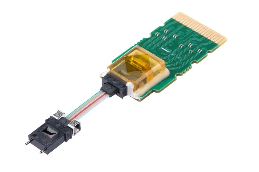
Figure 1: Multimode expanded beam fiber optic connection with polyetherimide resin optics and a multi-fiber ferrule connector.
High temperature operation must also be a consideration for manufacturers. At higher temperatures during everyday usage of the device, differences between the CTE of the lens material and that of any substrates with which the lenses are aligned can result in unacceptable signal losses. Common substrate materials include glass, silicon, and FR-4 composite.
Mechanical interlocks and adhesive glues are both used to assemble and align all components. Still, these can displace in different directions based on which parts are in contact and where they are located within the connector. The resulting interaction of these materials and their design constraints determines whether the parts meet optical tolerances or fail due to unconstrained expansion. Geometric constraints can limit these factors, and care must be taken to avoid creating stress that can cause subsequent cracking and reliability issues.
Another essential attribute to these optical materials is high heat resistance during the final product assembly of co-packaged optics — which involves reflow soldering at temperatures up to 260 °C. Thermoplastics that can withstand reflow soldering allow packaging to be performed after optical alignment. This significantly streamlines the assembly process.
Additional material requirements for optical lenses include manufacturability via rapid, high-volume production methods, such as multi-cavity micro-molding of thermoplastics, to meet requirements for surety of supply in critical data center infrastructure. For custom optical chips used within data centers, a broad design freedom is needed to create components that can handle huge data loads. Designs must also accommodate fixture integration to support alignment processes in automated assembly technologies, as well as pluggable connectors for repair options. Near-infrared (NIR)-transparent, injection-moldable thermoplastic polyimide resins with a glass transition temperature >280 °C and a relatively low CTE offer one solution that meets these requirements.
Toward a material solution
SABIC’s ULTEM resin is a polyetherimide material used in optical data center connectors and transceivers. The material offers a relatively low CTE and high stiffness, and it is widely used for multi-lens designs in custom optical components such as expanded beam fiber connectors. The material additionally features NIR transparency, a high refractive index, high modulus, and a lower CTE value compared to many optical thermoplastics.
These properties do not meet necessary thresholds to make the resin suitable for use as a lens material once the optics move closer to the ASIC. Although widely used for pluggable transceivers, the resin’s heat resistance is not sufficiently high to withstand typical reflow soldering for the board components.
To allow higher temperature solder reflow profiles to be used in co-packaged and onboard optics (JEDEC standard), SABIC developed EXTEM RH1017UCL resin. This thermoplastic polyimide material withstands the 260 °C peak temperature of PCB reflow soldering, significantly simplifying optoelectronic packaging and assembly. Testing revealed that typical coatings, such as anti-reflection coatings, showed good property retention after reflow soldering. The developed resin has remained stable during lifetime testing standards like Telcordia GR-468 for prolonged periods of hydro-aging.
Compensating for CTE mismatches
A thermoplastic polyimide resin, even with reflow soldering capability, does not offer maximum benefit compared to PCB substrate materials such as silicon and FR-4 composite — both of which offer lower CTE values compared to the developed resin. As mentioned, differences in CTE can cause optical components molded from thermoplastic to move out of alignment with the board under exposure to typical swings in use temperature that optics are prone to experience in a data center. These issues of alignment changes, part deformation, and/or material stresses must be addressed before resins like thermoplastic polyimide are to be used successfully for onboard and co-packaged optics.
Multiple approaches can be adopted to compensate for the issues raised by the higher CTE of the developed resin (50 ppm/°C) compared to those of substrate materials silicon (7-8 ppm/°C) and FR-4 composite (13 ppm/°C). Design adjustments to prevent misalignment issues offer one solution; mechanical fixations can create interlocking constraints that can be used to join a plastic component to an underlying part. This is shown in Figure 2: A 16-fiber expanded beam optic for the front face of a multi-fiber push on connector is joined to the underlying part using two metal pins. These multi-fiber push on pins help ensure dimensional alignment and prevent unwanted movement.
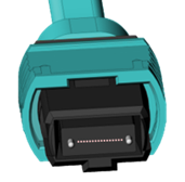
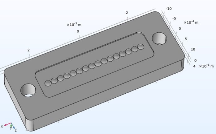
Figure 2. Top: a multi-fiber push on fiber optic connector used in optical fiber communication systems. Bottom: a 16-fiber expanded beam optic for the multi-fiber push on connector’s front face. The holes are mated with pins to align the fibers with the lenses.
Simulations of lens-to-lens distance changes under temperatures of 23-80 °C showed that the design with two fixation pins had a minimal misalignment of 0.2 µm between the lenses at the ends of the array and the substrate, yielding a strong coupling efficiency of 0.03 dB. This indicates that using fixation points on thermoplastic microlens arrays can help to retain critical alignment tolerances and thereby maintain dimensional stability and signal integrity (Figure 3).
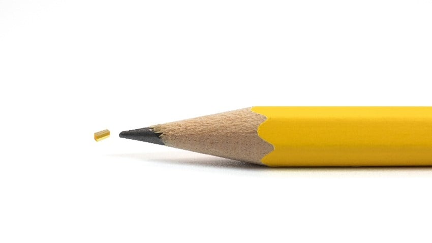
Figure 3: A microlens array made of EXTEM resin with 250-µm lens-to-lens pitch size, shown to scale.
Enabling a shift in optics
Production scalability is an additional consideration; to support the transition from plug-in optics to onboard and co-packaged optics, manufacturing at scale is critical to rapidly delivering the millions of required lenses and arrays at an affordable cost. To manufacture huge volumes of freeform and aspherical lenses, industry will require a material solution that offers compatibility with high-speed production methods such as multi-cavity injection molding and avoids time-consuming secondary operations such as grinding and polishing. Access to a network of micro-molders with proven experience in materials like thermoplastic polyimide is also essential.
Reaching the full potential of onboard and co-packaged optics now calls for the development of materials that not only deliver high performance and reliability, but that also support high-volume, high-speed production necessary to meet demand. Ultrahigh-heat thermoplastic polyimide resins have been shown to withstand the extreme temperatures of reflow soldering used in assembling onboard and co-packaged optics on the board.
However, a second challenge remains: managing dimensional changes and stresses that occur when various materials deliver different CTEs. Fortunately, design and processing optimizations can enable optical lenses and arrays made from thermoplastic polyimide resins to resist deformation and further advance the capabilities of data centers (Figure 4).
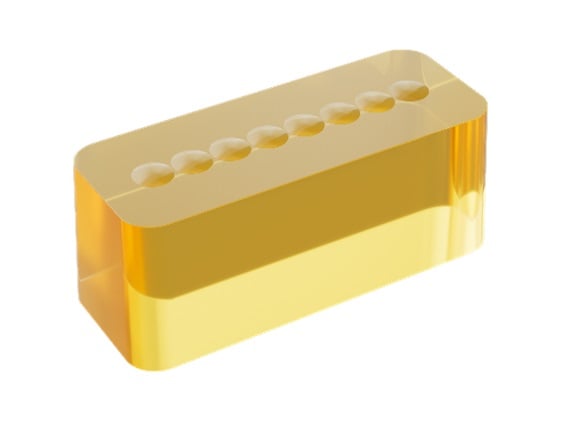
Figure 4: The microlens array (MLA) of EXTEM resin with 250-µm lens-to-lens pitch size.
While it is true that pluggable optics today remain dominant in fiber optic systems, massive increases in data transmission and storage are making onboard and co-packaged optics more appealing and viable options. These designs help boost bandwidth capacity, reduce latency, and cut power consumption compared to traditional pluggables. Simply, interchangeable optical assemblies (such as those in Figure 1) may achieve more scalable, modular designs as more components can be reflow soldered and easily packaged.