As demand for chips increases, vision system technology will be integral to inspection throughout the production cycle, from wafer development to packaging and testing.
Klaus Schrenker, MVTec Software GmbH
Despite the conventional notion that in certain regions of the global market investments in production capacity for semiconductor manufacturing have been curtailed, semiconductor production will remain vital — particularly in industrial settings that are reliant on developments in the digital revolution, such as AI. And according to the international consulting company McKinsey & Company, demand for semiconductors is rising and chips will need to be more efficient and compatible than ever, boosting the need to integrate machine vision into this production cycle.
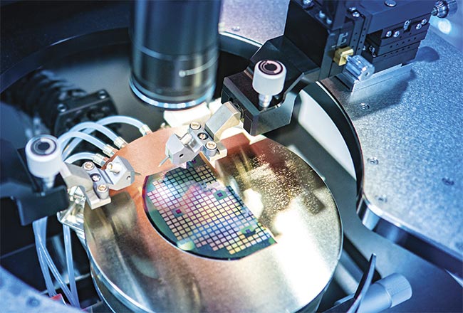
An industrial setting of semiconductor manufacturing. Courtesy of Grispb/stock.adobe.com.
According to Bain & Company’s Technology Report 2024, the demand for certain upstream semiconductor components, such as materials and software, will increase by at least 30% by 2026 due to the AI-driven demand for graphics processors. Semiconductor production will therefore remain extremely important and continue to grow over the long term. This article will explore the activities and processes in which machine vision already plays an essential role in ensuring the efficient production of semiconductors, and the added value it brings.
Production cycle monitoring
Few system components involve
as many benchmarks in their production as semiconductors. Ranging from wafer production and other front-end processes to advanced packaging and back-end operations, such as testing, hundreds of different steps are required, making the implementation and coordination of these stages complex and sensitive. This complexity calls for technologies that can be used and adapted quickly during specific steps of each cycle, while boosting production efficiency.
Machine vision technologies play a key role in monitoring these various steps. And machine vision systems enable numerous inspection and alignment processes to be performed automatically and with high precision — both of which are critical for semiconductor manufacturing. Moreover, a majority of the front-end processes such as photoresist coating, photolithography, and etching must be repeated 40 to 100 times, making the repeat accuracy of these technologies a crucial factor. To address these demands, robust and advanced machine vision software is used to implement applications such as defect detection, measurement, and matching and alignment, which provide significant advantages at various production stages.
Machine vision ensures quality
In nearly every stage in semiconductor manufacturing, any functional or optical defects must be checked and potentially addressed. Given the multi-week duration and high complexity of the entire manufacturing process, it is crucial to monitor the components’ quality continuously. Detecting defects early — and not after sophisticated and costly manufacturing steps have been carried out — can make a significant financial difference to a producer’s bottom line. Using machine vision to automatically perform this quality control offers many advantages compared with manual or alternative inspection methods. Machine vision systems are not only much faster but also deliver objective and reproducible results.
Detection of a microscopic defect on a wafer. Courtesy of MVTec Software GmbH.
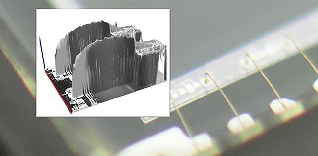
The depth from focus method can be used to check the courses of the wires. Courtesy of MVTec Software GmbH.
Unlike manual inspections, the performance of machine vision systems is not at risk of deteriorating due to fatigue or lack of alertness in monotonous tasks. Additionally, AI-powered deep learning technologies address this: Deep learning-based anomaly detection enables automated surface inspections, including the identification of irregularities, and provides the foundation for subsequent defect
segmentation. These are applications that were previously impossible prior to the integration of deep learning methods.
In terms of overall quality control, determining the dimensional stability of a semiconductor is just as essential as detecting any inherent defects. Machine vision can measure edges along lines or circular segments with subpixel accuracy in a matter of milliseconds. In addition, 3D measurement enables the reconstruction of disparity images, distance images, or 3D surface coordinates using advanced techniques.
Aside from quality inspection, machine vision can be applied for purposes of finding and aligning wafers, layers, and chips. This primarily involves the use of subpixel-precise shape matching. This technology finds objects contained in an image precisely and robustly, in real time. This holds true even under challenging conditions, such as when objects are rotated, scaled, distorted in perspective, locally deformed, partially obscured, or positioned outside the image frame.
Front-end and back-end processes
Roughly speaking, the production process for semiconductors is divided into front-end and back-end steps.
During front-end production, chemical and physical processes are applied repeatedly to a substrate, i.e., a silicon wafer, to build microelectronic circuits layer by layer. After this, in the back-
end production, the individual wafers are separated and contacted, fitted with a housing, and prepared for use. Machine vision systems offer a wide range of technologies that can be
used in a multitude of ways in both front-end and back-end production.

Redistribution layer (RDL) inspection. Adapted with permission from Reference 1. Courtesy of MVTec Software GmbH.
In front-end production, machine
vision’s key application — as well as one of its specialties — is in defect detection. An example could be the robust detection of a wide range of defects on the surface of a wafer.
Machine vision technologies working
at various dimensions identify microscopic cracks, scratches, and particle contamination on the wafer surface, ensuring quality and cycle time requirements. Sophisticated machine vision software can even work in difficult lighting conditions and on complex backgrounds. Driven by such software, the analysis and quantification of all kinds of defects can inform deep learning-based anomaly detection, or a conventionally trained variation model. For maximum speed and performance, a combination of rules-based algorithms and AI methods is often recommended.
Another widely implemented use of machine vision is the reading of characters and codes. In semiconductor production, optical character recognition (OCR) and 2D data matrix code reading allow the identification and tracking of wafers throughout the production process. Certain marks typically include batch numbers, production dates, manufacturer codes, and other information. Such seamless traceability is essential for automating the many complex production steps reliably and quickly. A technology particularly effective for these applications of the semiconductor industry is Deep OCR. The name comes from the powerful deep neural networks that it is based on. Deep OCR offers significantly higher accuracy and improved ease-of-use compared with conventional OCR solutions. It even recognizes whole words by grouping characters, reducing errors caused by the misinterpretation of similar-looking characters.
The inspection of redistribution layers (RDLs) is another critical application. RDLs are an advanced packaging technology that allow efficient interconnections between the chips and other components. The integrity and quality of the RDL usually needs to be inspected in the micrometer range to ensure compliance with design specifications. Here, stable and accurate pattern matching methods based on a collected data set come into play. They enable precise alignment of the respective components and can measure 2D structures with subpixel accuracy (up to 1/50 pixel can be required, depending on the application).
Of course, for these use cases, machine vision engineers select the algorithms and methods that work best for the respective inspection setup and object. Generally speaking, it is recommended to use machine vision software that provides a platform able to implement methods for solving all kinds of applications at various stages of the process.
As production progresses, machine vision is also vital for measuring so-called wafer bumps, which are protruding, metallic solder balls that are attached to the wafer. These bumps ultimately serve as the connection between the chip and the circuit board, for example. Their precise height, diameter, and the overall uniformity of the structures are vital to ensure flawless functionality and reliability. Three-dimensional image processing technologies, such as 3D surface inspection, shape-based 3D matching, and 3D measurement, can be used to inspect and measure these bumps.
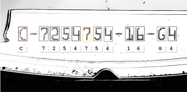
Optical character recognition (OCR) on a component. Courtesy of MVTec Software GmbH.
Machine vision also provides support for the so-called prober testing, in which the wafers’ circuits are tested with electrical prober needles or probe cards. Due to the microscopically small structures on the wafer, microscopes generate the necessary images; two microscopes are often required to cover the wafer surface with sufficient resolution. Exact alignment with high accuracy is crucial for this delicate testing method to be conducted correctly. Furthermore, if the wafer is not aligned properly, the probe needle could damage it and thus destroy the wafer completely.
So, machine vision technologies are used here as well, in two iterations: First, the inclination is determined by establishing the focal plane; cameras in both microscopes capture an image, and then the two are compared. If both images have the same sharpness, the wafer is properly aligned. If not, the machine readjusts until both images are equally sharp. In the second step, the system checks whether the wafer is aligned flush or has rotation. For these tasks, the shape-based matching method is the best choice for a manufacturer. The known distance between the two camera positions is used to determine the displacement and rotation in relation to the center of the axis between the left and right images. If necessary, the wafer’s position is corrected.
Machine vision can also support back-end production. One crucial application is wire bonding. This process involves connecting wires to the pads, i.e., the contact points of the precisely separated parts of a wafer (dies), and to the lead frames on the housing. Machine vision systems help align dies within their housings and inspect the bonding process for potential defects, such as insufficient wire contacts, incorrect cut length, or improper bonding pressure.
During inspection, the pads are first located in the image. This is the first step in narrowing the relevant areas for examination. Then, machine vision segmentation methods are used to locate the wires in the image. Based on these two pieces of information, the system can determine whether the minimum overlap has been achieved and verify whether the wire is properly connected to the relevant contact area of the lead frame.
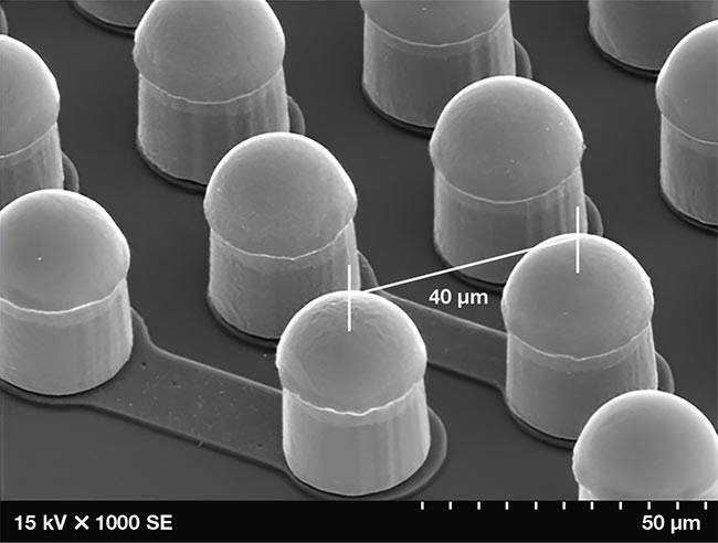
Wafer bumps under magnification, which serve as the connection between the chip and circuit board. Adapted with permission from Reference 2. Courtesy of Courtesy of MVTec Software GmbH.
Bond inspection is a well-established quality control process, especially when packaging the chip. It requires the utmost precision to evaluate the position of the wire and the integrity of the bond at a microscopic level. Machine vision technologies use 2D and 3D measurements for this purpose. They reliably detect the slightest gaps and positional deviations, even against complex backgrounds.
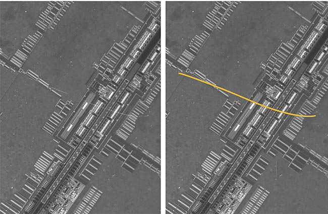
After bonding, the wires must be inspected. This is a major challenge due to difficult lighting conditions, such as reflections on surfaces. However, using machine vision software, the wire trajectories can be reliably inspected, even if adequate illumination is unavailable. First, the start and end points of the wires are extracted using blob analysis. Then, the regions of interest are reduced by the software to the area between these points. Finally, sophisticated line detection algorithms are applied to identify the wires, even in dark areas where their exact locations are nearly invisible.
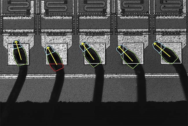
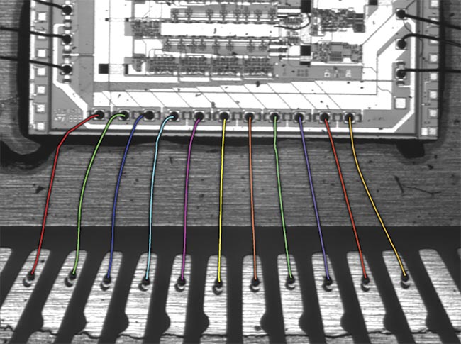
Bonding connections (top) and cables (bottom) are detected accurately. Courtesy of MVTec Software GmbH.
Furthermore, the 3D trajectory of the wires must be checked. Specifically, it is necessary to determine whether each wire lies within its designated 3D corridor. For this purpose, the image processing method called depth from focus is ideal; this is a technique where 3D structure is calculated by analyzing pixels captured at different focal distances.
Another key back-end application is 3D flip chip measurement. Flip chip bonding is an assembly and connection method to contact unhoused semiconductor chips. It involves directly connecting the face-down integrated circuit chips onto substrates or circuit boards, using conductive bumps on the chip’s surface. Similar to wafer bump inspection, the accurate 3D measurement of these bumps is vital for device performance and reliability. For this purpose, state-of-the-art point cloud processing algorithms are employed. These enable measurements such as coplanarity checks or level sections through the bumps.
The previously described uses are just a few of many examples of how cutting-edge machine vision technologies are optimizing semiconductor manufacturing. The potential for machine vision in this industry is vast, with countless other use cases on the horizon. As the demand for faster, smaller, and more powerful devices grows, machine vision will continue to play an indispensable role in driving innovation and ensuring quality in semiconductor manufacturing — now and into the future.
Meet the author
Klaus Schrenker joined MVTec in 2021. As business development manager, he is responsible for the strategic business development across all products as well as the evaluation and development of new business areas and applications; email: [email protected].
References
1. B. Sawyer et al. (2015). Design and demonstration of 40 micron bump pitch multi-layer RDL on panel-based glass interposers. IMAPSource Proc, Vol. 2015, No. 1, pp. 379-385.
2. R. Parthasarathy and U. Tosun. (2023). Defluxing of copper pillar bumped flip chips. Proc IMAPSource, Vol. 2023, No. DPC, pp. 438-482.