Long-distance, high-speed communication depends on lasers to provide the optical power source. But this application is becoming more and more demanding, especially in terms of power consumption, price and bandwidth.
With ever-increasing demands on bandwidth, speed and deployment, efforts to reduce the size and cost of communications systems have never been so important.
One technology that has continued to keep pace with demand so far is the semiconductor laser, but can it continue to evolve to provide optical communications systems with higher speed, lower production costs, lower power dissipation and a smaller form factor? Opinions are mixed.
“In optical systems, the laser itself cannot be shrunk; its size is dictated by physics,” said Martin Zirngibl, head of Physical Technologies Research at Bell Labs in Murray Hill, N.J. “However, you can more tightly integrate everything that is needed to operate the laser.”
Optical systems contain footprint-consuming packaging that includes electrical, optical and optoelectronic components, all of which must work together.
“You have to send light from one component to another; these interconnections take up a lot of real estate,” Zirngibl said, “so one very important technology for shrinking optical components is integration of multiple functionalities onto a single chip. This eliminates the interconnections. The components still have the same size, but they are put very closely to each other.”
Laser technology must be improved
While there are techniques and design advances that have evolved to keep pace with our needs, next-generation technology must step up its game.
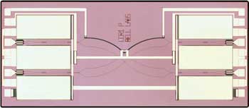
This silicon photonics integrated circuit comprises dual polarization and a dual-quadrature coherent receiver. Courtesy of Alcatel-Lucent.
Techniques such as wavelength division multiplexing allow a number of optical signals to be communicated over a single optical fiber by using different wavelengths of laser light. In addition, devices can be designed with well-controlled and narrow lasing linewidths, thus minimizing the effect of fiber dispersion. This allows multiple wavelengths to be carried in the same fiber without interference between the channels.
But to keep up with increasing demand, laser manufacturers must increase the speed of lasers and decrease the size of components – at the same time, crucially, bringing down costs.
Today’s fiber optic transmission relies on two basic semiconductor laser configurations: edge emitters and vertical-cavity surface-emitting lasers (VCSELs). As their names suggest, edge emitters are designed to emit light parallel to the plane of the wafer surface, whereas VCSELs emit light perpendicular to the surface of the wafer.
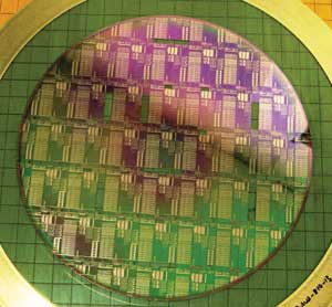
An 8-in. wafer of silicon photonic chips. Courtesy of Alcatel-Lucent.
Edge emitters such as Fabry-Perot lasers are commonly used in short-reach, low-speed applications, while distributed feedback (DFB) lasers emit a narrower spectral linewidth – useful for long-reach applications.
But it is the VCSEL that some say is the most promising candidate for future communications systems. It was invented in the late 1970s and quickly gained popularity for use in short-reach applications such as fiber channel, Ethernet and intrasystems links. By the end of the 1990s, VCSELs had become the technology of choice for short-range datacom, effectively displacing edge-emitter lasers.
As in all semiconductor diode lasers, layers of semiconductor material are grown on top of each other on a substrate known as the epi. In a VCSEL, the active layer is sandwiched between two highly reflective distributed Bragg reflectors. The VCSELs can be designed for top emission (at the epi-air interface) or bottom emission (through a transparent substrate).
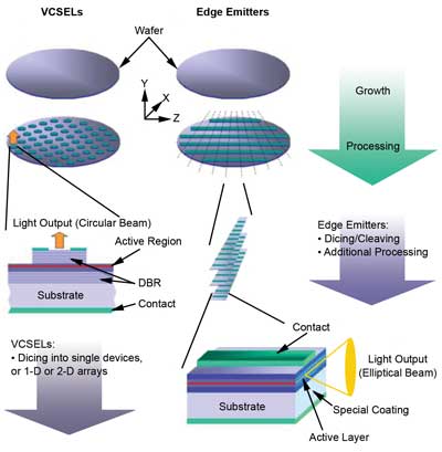
Comparison of the growth/processing flow of VCSEL and edge-emitter semiconductor lasers. Courtesy of Princeton Optronics.
Today’s VCSELs are cheaper to produce than edge emitters and can be used for higher-speed fiber optic communication over short or long ranges.
Researchers at the Swiss Federal Institute of Technology in Lausanne (EPFL) have been working on the science and technology of low-dimensional semiconductors (semiconductor quantum wells, wires and dots) and photonic nanostructures (micro- and nanocavities, photonic crystals), as well as wafer-fused long-wavelength VCSELs.
BeamExpress SA, an EPFL spin-off company, was launched to manufacture long-wavelength VCSELs for telecom applications. The company delivers low-power-consumption VCSELs with wavelengths ranging from 1250 to 1650 nm and data rates up to 10 Gb/s.
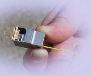
Wavelength-division-multiplexed VCSEL modules are used in high-bandwidth optical fiber communications systems. Courtesy of BeamExpress SA.
“With traffic in optical networks increasing exponentially, the need for power saving has emerged as a key constraint limiting industry growth and profitability,” said professor Eli Kapon, founder and chief scientist at BeamExpress SA and director of the Laboratory of Physics of Nanostructures at EPFL.
“Due to the energy inefficiency and associated cooling requirements of existing DFB and Fabry-Perot laser sources, the physical footprint of higher speed and higher density fiber optic transmission equipment threatens to become impractical,” he added. “Further, electricity consumption in optical networks has become a significant operating cost as well as an ecological challenge.”
VCSELs: The future of optical transmission?
By their very nature, VCSELs are dramatically more energy-efficient optical sources than either DFB or Fabry-Perot lasers. A drawback, however, is that they do not have very high single-mode power, so they have to be used with amplifiers to boost their power for high-speed communications.
VCSELs operating in the visible and short-wavelength-infrared spectral regions (850 nm) have found broad and successful applications in a variety of manufactured products, including computer mice and automotive control components.
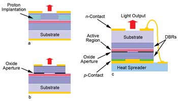
Three common types of VCSEL structures: (a) a top-emitting structure with proton implantation to confine the current, (b) a selectively oxidized top-emitting structure to confine the optical modes and/or the current, and (c) a mounted bottom-emitting selectively oxidized structure. Courtesy of Princeton Optronics.
But producing VCSELs that operate at the longer wavelengths necessary for fiber optic communications has been a fundamental challenge due to physical constraints imposed by the semiconductor materials that make them up, Kapon said.
The constraints are for growing the epitaxial materials for VCSELs such as distributed Bragg reflector mirrors and quantum wells – which are very difficult at 1550 nm – but are overcome with BeamExpress wafer fusion technology, Kapon claims.
“The VCSEL wafer-fusion technology licensed to and developed by BeamExpress in cooperation with EPFL is uniquely suited to overcome these constraints, and allows efficient manufacture of VCSELs operating in the 1300- to 1550-nm-wavelength range necessary for fiber optic communications,” he said. “Compared to DFB and Fabry-Perot lasers operating in the same applications, the increased energy efficiency of long-wavelength VCSELs enables significant reduction in both component footprint and power consumption.”
The multimode 850-nm VCSEL has been massively adopted by the industry and is used in 95 percent of all optical networking applications at the short reach (less than 100 m) and medium reach (less than 1000 m).
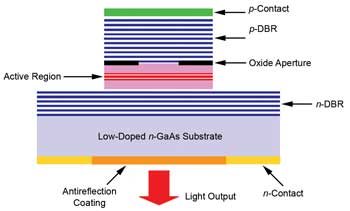
Schematic of a selectively oxidized, bottom-emitting 1064-nm VCSEL diode laser structure. Courtesy of Princeton Optronics.
VCSELs that can reach 10 Gb/s already are being used for short-range communications, and in the future, the speed can be increased to 40 or even 100 Gb/s, according to New Jersey-based VCSEL manufacturer Princeton Optronics Inc.
“Lasers are used for different applications; one is long haul in trunk routes. For that, people use tunable lasers from companies like JDS, Santur, etc.,” said Chuni Ghosh, chief technology officer at Princeton Optronics Inc. “For data communication and short-range communication, people use VCSELs from companies like Finisar and Emcore.”
While Princeton Optronics Inc., which sells VCSELs for high-power applications, does not currently sell products in the data communications market, it is planning to enter the market next year with its high-efficiency, high-power datacom VCSEL products.
“Princeton Optronics’ high-speed VCSELs have higher power and higher efficiency,” Ghosh said. “For example, our single-mode lasers deliver power levels of 4 to 30 mW, compared to the single-mode power of the rest of the industry of 1 mW or less. In terms of efficiency, our devices deliver efficiencies of >45 percent compared to the rest of the industry’s number of <20 percent.”
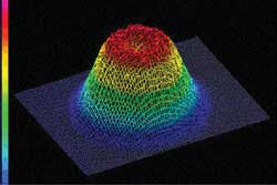
Far-field beam profile of a 5 x 5-mm VCSEL array at 100-W output power; however, the same shape can also be obtained from a single device. Courtesy of Princeton Optronics.
Of course, some believe that the Holy Grail lies in the realization of silicon photonics – a pursuit that Intel is furiously working on. Silicon photonics would allow unprecedented integration and would reduce cost, Kapon commented.
But Bell Labs’ Zirngibl points out one major deficiency: You cannot make a laser out of silicon. What’s more, the fundamental size of various components is pretty much the same whether they are on silicon or indium phosphide.
“One advantage silicon photonics has is that there is a huge embedded manufacturing base. So scaling any solution to large-volume production is pretty easy. The dream would be to run photonic devices just like you do CMOS today, but we are still far away from that,” he said. “One other advantage could be that you could easily integrate a lot of electronics around your optical devices. In current transmitters and receivers, this is not really necessary, but it could open up new applications.”
Zirngibl and colleagues are trying to build sources on silicon by attaching pieces of III-V laser material onto silicon wafers. The “combo” wafer is then processed in a single step that constructs the laser and electronics simultaneously.