Search
Menu
OSI Optoelectronics - Custom Solutions LB 5/23
Photonics HandbookIndustry News

Jenoptik Opens Dresden-Based Micro-Optics Fab

Facebook X LinkedIn Email
The Jenoptik Group has completed its micro-optics fabrication site in Dresden, Germany, combining all former operations in the city. Representing an investment of just under €100 million ($113.7 million), the factory employs almost 100 people on a total net floor space of 11,000 sq m, including 2000 sq m for production in ISO 5 and ISO 3 clean rooms. The new location also offers expanded production capacities for micro-optics and micro-optical sensors used in systems for semiconductor lithography and inspection and laser material processing.

According to Saxony's minister president Michael Kretschmer, the facility is expected to contribute to the semiconductor ecosystems of Germany and of Europe as a whole, as well as to European technological sovereignty.
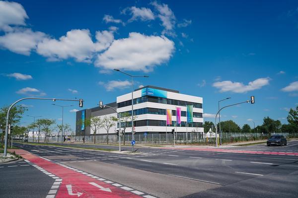
Jenoptik's new micro-optics facility in Dresden, Germany. Courtesy of Jenoptik.

In addition to Dresden, Jenoptik manufactures high-precision and micro-optics at its sites in Jena and Triptis, Germany, in Heerbrugg, Switzerland, and in Jupiter, Fla. and Huntsville, Ala. The company employs around 4600 people worldwide.
Lambda Research Optics, Inc. - One Day Coating Service


Published: May 2025
Glossary
micro-optics
Micro-optics refers to the design, fabrication, and application of optical components and systems at a microscale level. These components are miniaturized optical elements that manipulate light at a microscopic level, providing functionalities such as focusing, collimating, splitting, and shaping light beams. Micro-optics play a crucial role in various fields, including telecommunications, imaging systems, medical devices, sensors, and consumer electronics. micro-optics suppliers → Key...
lithography
Lithography is a key process used in microfabrication and semiconductor manufacturing to create intricate patterns on the surface of substrates, typically silicon wafers. It involves the transfer of a desired pattern onto a photosensitive material called a resist, which is coated onto the substrate. The resist is then selectively exposed to light or other radiation using a mask or reticle that contains the pattern of interest. The lithography process can be broadly categorized into several...
Businessexpansionsfactoriesmicro-opticssemiconductorsindustrialmanufacturingSensors & Detectorslithographyinspectionmaterials processingEuropeJenoptikIndustry News

We use cookies to improve user experience and analyze our website traffic as stated in our Privacy Policy. By using this website, you agree to the use of cookies unless you have disabled them.