
Innovative Optical Lithography Advances High-Resolution Semiconductor Laser Production
Displacement Talbot lithography is positioned to support the next generation of semiconductor laser designs and their development.
By Kelsey Wooley, Zhixin Wang, and Harun Solak
The rapid advancement of AI, driven by large-language models, is creating unprecedented demand for computational power. This surge has in turn placed tremendous pressure on the underlying physical hardware, such as optical communication modules in data centers.
Within these modules, semiconductor lasers such as distributed feedback (DFB) lasers and VCSELs are fundamental components. The durability and performance advantages of these lasers extend beyond data communications into a wide range of applications, including lidar systems used in advanced driver-assistance systems,
mobile devices, and analytical applications.
Courtesy of iStock.com/kynny.
A common feature in these high-performance lasers is the use of high-
resolution periodic structures, which
enable these lasers to achieve stable
single-mode operation, polarization control, surface emission, and other features of interest. The use of high-resolution periodic structures also enables beam
engineering, which further optimizes these sources for numerous applications.
The adoption of these high-resolution structures necessitates a suitable patterning solution for high-volume manufacturing — and fabricators currently have several options. Predictably, each has advantages and drawbacks. Electron-beam (e-beam) lithography, for example, offers ample resolution and good yield. However, the technique is too slow for large-area volume production. Projection lithography, though well established, is often prohibitively expensive in terms of equipment purchase and maintenance. Nanoimprint lithography provides higher throughput than e-beam, but its quality
is susceptible to defects and it faces challenges with yield, overlay accuracy, and limited master lifetime. Meanwhile, interference lithography offers acceptable resolution but is limited by low throughput. Further, the difficulty of achieving precise control of the wavefront and pitch makes uniform, large-area patterning a challenge.
As a result, a cost-effective, high-throughput solution for patterning high-resolution periodic structures with robust quality is a coveted advancement in the semiconductor laser industry.
Displacement Talbot lithography (DTL) offers a promising alternative to currently deployed lithographic technologies, providing an economical path for the industrial production of high-resolution patterns. A distinctive imaging principle characterizes this method, which enables an effectively unlimited depth of focus that can reach millimeter-level values — and in some cases, values of several millimeters (Figure 1).
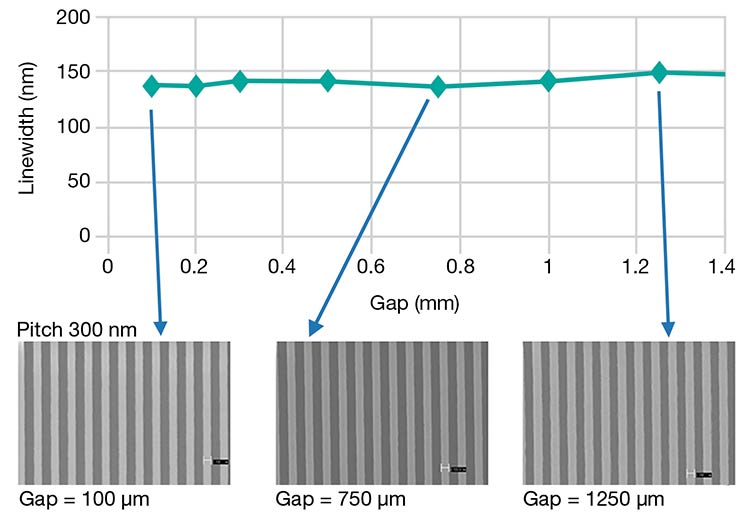
Figure 1. Displacement Talbot lithography (DTL) offers an effectively unlimited depth of focus that can reach several millimeters. Shown above are microscopy images of 300-nm-pitch gratings at different exposure gaps. The target linewidth is 150 nm. Courtesy of Eulitha AG.
Further, DTL has an extremely large single-exposure field — up to 140 × 140 sq mm when used with the most commonly available 6-in. photomasks — with excellent pattern uniformity and pitch accuracy. The pitch uniformity has been characterized in the single-digit picometer range across a full wafer. In addition, the absence of complex objective lenses between the photomask and the wafer, combined with a noncontact exposure process, gives DTL a low cost of ownership and maintenance, especially compared with its high resolution, which can reach up to 60 nm (half-pitch) for printing periodic gratings.
As an optical lithography approach that is mature and well established in the semiconductor industry, DTL fits smoothly with industry-standard materials, including photomasks and photoresists.
DTL for laser manufacturing
DTL’s principal advantages are its high throughput and cost effectiveness. The method simultaneously overcomes the throughput issue that hinders e-beam lithography and the cost limitations of projection lithography.
Additionally, it provides the robust, large-area patterning that nanoimprint and interference lithography struggle to guarantee. This advantage becomes even more pronounced as the laser industry transitions to larger wafer sizes, up to 6-in. and beyond in certain cases.
DTL also offers high repeatability, which is a critical quality for high-volume production. Typically, laser devices are defined in small areas, spanning tens to hundreds of micrometers. With DTL, this can be easily achieved through an additional step of low-resolution lithography to define these areas. Repeatability is then guaranteed by the use of a noncontact photomask.
Moreover, at a time when numerous distinct integrated photonics material platforms are evolving and advancing, DTL is compatible with indium phosphide, gallium arsenide, silicon carbide, gallium nitride, silicon, glass, and other substrate materials currently of interest.
VCSELs: Enhancing performance
In terms of aligning the capabilities of DTL with laser system architectures, VCSELs represent a compelling, well-matched application. These lasers are widely used in consumer lidar, optical communication, and face-recognition
systems, and they have demonstrated utility in many other applications.
To further optimize VCSEL performance, designers may include high-
resolution gratings in advanced VCSEL devices for polarization control and/or beam engineering, or as a high-reflectivity mirror within the laser cavity. In this example, a typical fabrication flow
involves using DTL to pattern the high-resolution grating across the wafer, followed by a second, low-resolution exposure to define the individual laser cell boundaries. This results in sharply defined grating areas (Figure 2).
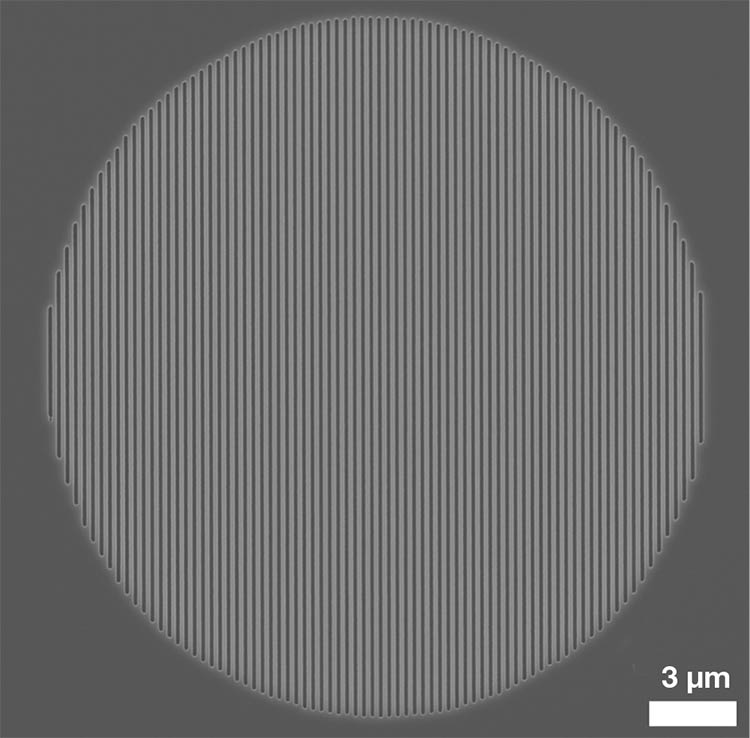
Figure 2. A typical VCSEL cell with surface gratings. The high-resolution grating, with a 280-nm pitch, is patterned using DTL, and the 22-µm circular boundary is sharply defined in a subsequent low-resolution lithography step. Courtesy of Eulitha AG.
The success of this method is well documented, and the supported applications are diverse. For example, DTL-
manufactured VCSELs have demonstrated an orthogonal polarization suppression ratio (OPSR) of 30 dB1. This effort opens the door to precision timekeeping use cases and doubled-data-rate polarization-multiplexed free-space links1. Meanwhile, another study concluded that DTL exposure technology could be implemented instead of e-beam lithography exposure technology to yield surface periodic gratings2. This success has led major VCSEL foundries in Asia to adopt DTL for 6-in. wafer production, positioning it as a key technology for next-generation optoelectronic devices.
Bolstering spectral performance
DFB lasers, as well as distributed Bragg reflector (DBR) laser diodes, represent another core application for DTL. These laser architectures rely on DTL technology to produce gratings with exceptional pitch accuracy — <10 pm across the exposure field. This level of precision is critical for the spectral performance of these laser sources. In addition to its unmatched pitch control, DTL offers the advantage of patterning directly over wafer topography, enabling integration into complex device architectures. DTL covers a wide pitch range, from ~120 nm to >1 µm, making it suitable for lasers from the visible (blue) to the infrared spectrum.
A notable feature of many DFB lasers is the inclusion of a quarter-wave phase shift for stable single-mode operation. Traditionally, this phase shift is introduced abruptly by modifying a single grating period. DTL provides an equivalent solution by implementing a gradual phase shift over several grating periods, which accurately achieves the same total phase shift value. Figure 3 shows a schematic of the phase profile. Preliminary results demonstrate that this approach achieves performance comparable to conventional designs.
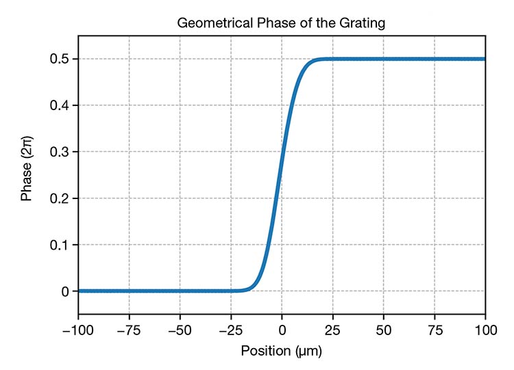
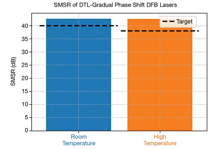
Figure 3. The phase profile of a gradual phase-shift design compatible with DTL exposure (top). The total phase shift is precisely defined as π, which inverts the relative location of the grating lines. Experimentally measured single-mode suppression ratio (SMSR) for distributed feedback (DFB) lasers patterned with DTL and incorporating the gradual phase-shift design (bottom). The SMSR values exceed the device target at both room and high temperatures. Courtesy of Eulitha AG.
Devices fabricated via this method
exhibit an average single-mode suppression ratio of 42.65 dB at room temperature and 42.57 dB at high temperature for a grating pitch of ~203 nm (Figure 3). With further iteration and optimization of the phase-shift design as well as the subsequent process control, a higher single-mode suppression ratio and yield should be expected.
Next-generation sources
Photonic crystal surface-emitting lasers (PCSELs) are an emerging class of semiconductor lasers offering high power and single-mode surface emission in a narrow beam3. These qualities make these lasers a promising solution for lidar, on-chip communication, and other fields. Unlike DFB lasers, PCSELs are patterned with 2D periodic arrays, typically arranged in square or hexagonal lattices. The lattice constant is proportional to the emission wavelength.
DTL, which can be used to print not only 1D gratings but also 2D periodic arrays, offers a compelling combination of large-field exposure and unlimited depth of focus (Figure 4) for this manufacturing application. As PCSELs move toward high-volume production and greater market presence, DTL provides a clear path to robust and economical manufacturing.
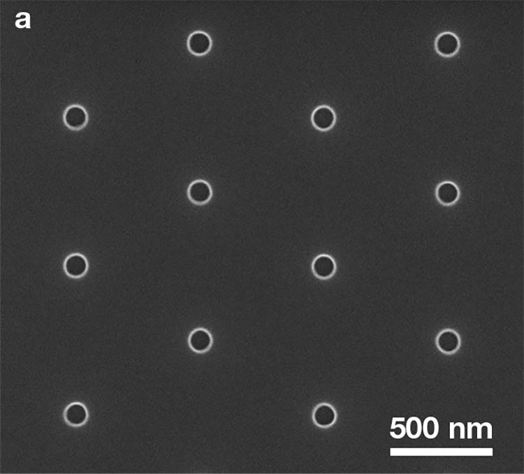
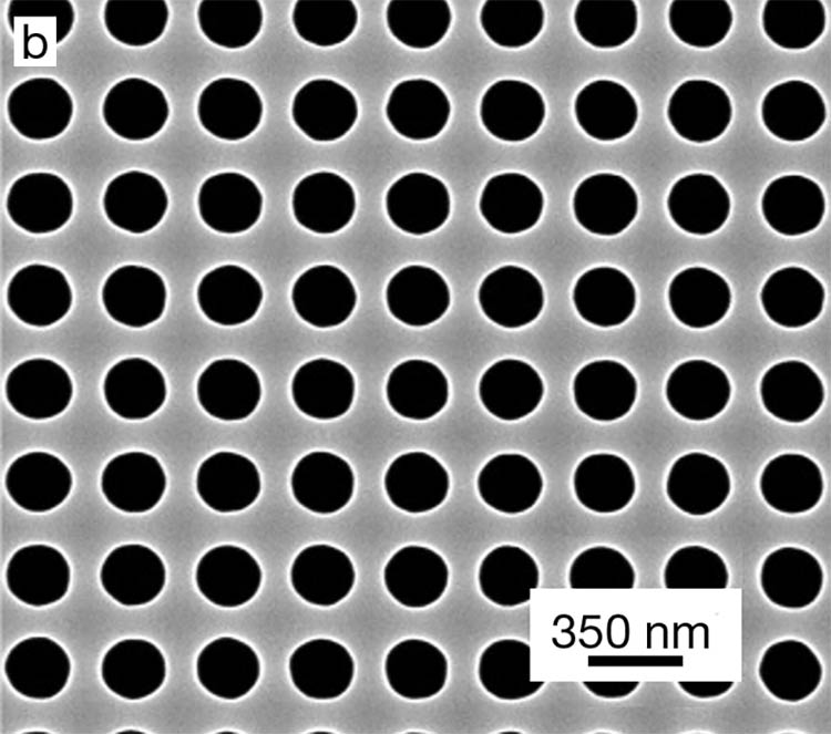
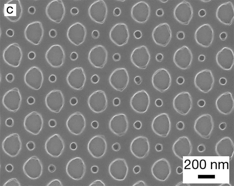
Figure 4. Representative microscopy images of 2D periodic patterns fabricated using DTL. Circular holes in a hexagonal lattice (a). Circular holes in a square lattice (b). A double-hole square lattice (c). Images (a) and (c) are adapted with permission from Reference 4. Courtesy of Eulitha AG.
Future outlook
By overcoming the limitations of conventional methods, DTL delivers an unmatched combination of high resolution, exceptional pitch accuracy, large-area uniformity, and economical cost. Its unlimited depth of focus allows patterning over complex wafer topography, and its compatibility with standard fabrication processes ensures seamless integration into current production lines.
As demand for high-performance lasers continues to grow, DTL is well positioned to become an industry standard for the next generation of semiconductor laser production.
Meet the authors
Zhixin Wang leads the Computational Lithography team at Eulitha AG in Switzerland. He earned bachelor’s and master’s degrees from Peking University and a Ph.D. from ETH Zürich; email: zhixin.wang@eulitha.com.
Kelsey Wooley is director of Eulitha U.S. and leads global application initiatives. She graduated with a degree in chemical engineering from Brigham Young University and has worked at Intel, Micron, and Meta’s Reality Labs; email: kelsey.wooley@eulitha.com.
Harun Solak is cofounder and CEO of Eulitha AG. He received a Ph.D. in electrical engineering from the University of Wisconsin. As a staff scientist at the Paul Scherrer Institute, he helped set up the first extreme-ultraviolet interference lithography systems; email: harun.solak@eulitha.com.
References
1. Y. Liu et al. (2018). OPSR enhancement
of high-temperature operating shallow-surface grating VCSELs. Appl Opt, Vol. 57, No. 16, pp. 4486-4490.
2. Z. Shi et al. (2023). High throughput
fabrication of surface gratings on VCSEL using displacement Talbot lithography.
Proc SPIE, Vol. 12556, Beijing, China.
3. K. Hirose et al. (2014). Watt-class high-power, high-beam-quality photonic-crystal lasers. Nat Photonics, Vol. 8, pp. 406-411.
4. S. Rietmann et al. (2025). Enhancing displacement Talbot lithography through inverse-designed curvilinear masks and multibeam mask writing. Proc SPIE,
Vol. 13424, 134240G, San Jose, Calif.
/Buyers-Guide/Eulitha-AG/c30797