JUE WANG AND INDRAJIT DUTTA, CORNING INCORPORATED
The rapid growth of advanced and intelligent technologies that power our daily lives — including hyperscale data centers, artificial intelligence, and smarter consumer electronic devices — is fueling the demand for more computing power and requiring even more powerful semiconductor chips. Driven by the need to support the rate at which this exponential technological growth is occurring, industry is adopting new photolithography tools that can print chips faster and with smaller features.
Amid semiconductor manufacturers aiming to realize higher throughputs and extend the lifetime of deep-ultraviolet (DUV) lithography systems, the use of an optimal material, as determined by the application, can in turn be a key determinant of performance, cost, and durability (Figure 1). Printing chip circuits at this scale demands an extremely precise laser as well as durable supportive optics. To meet these requirements, the selection of material is a critical consideration.
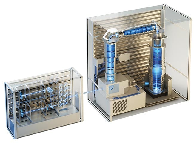
Figure 1. An argon fluoride
(ArF) excimer laser/deep ultraviolet
(DUV) lithography
system setup, representing
a traditional lithography
system setup for the
semiconductor industry.
Historically, industry has favored argon fluoride (ArF) excimer lasers in and for lithography systems for the semiconductor industry. Recent improvements to these DUV sources have increased power levels from 60 to 90 W, and up to 120 W. The nanosecond-pulsed lasers operate at a wavelength of 193.4 nm, which corresponds to a photon energy of 6.42 eV1.
Owing to high fluency, excellent lifetime stability, and high damage threshold in the DUV, crystalline materials — for example, calcium fluoride (CaF2) — have been widely considered the materials of choice for ArF laser-based microchip fabrication.
Low-loss and laser-durable CaF2
In recent years, semiconductor industry partners increasingly demanded higher-UV photon energies, longer pulse lengths, improved speckle performance, and higher pulse power densities to print more chips. CaF2 laser windows and other optical materials were unable to meet necessary performance requirements, because these materials were becoming damaged after short exposure times.
In this context, an optimized material supporting low-loss and laser-durable CaF2 laser windows was needed to support the next generation of high-powered lasers2. Corning Incorporated, with a history of growing CaF2 ingots, developed a CaF2 material for microlithography and laser optics applications that offers advantages compared with the previous materials. Additional research was subsequently dedicated to improving surface finishing, preparation, and coatings, which play a critical role in both the lifetime and optical performance of CaF2 laser windows. Subsurface damage-free surface finishing and protective coatings extend the lifetime of CaF2 laser windows by several orders of magnitude.
Laser and plasma coloration
Obtaining a fundamental understanding of the interaction of high-energy photons with CaF2 optics is critical for improving the durability of these laser optics. ArF laser-induced damage of CaF2 is associated with metallic calcium (Ca)-colloid formation. This is shown in Figure 2, in which the bulk surface Ca-colloid absorption leads to a purple appearance. The laser coloration is the result of a combination of the laser interaction with CaF2 surface and bulk and a broadband absorption between 520 and 580 nm1.
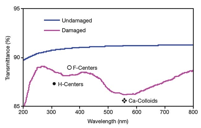
Figure 2. Spectral transmittance of argon fluoride (ArF) laser-damaged calcium fluoride (CaF2), indicating absorptions associated with calcium (Ca)-colloids, F-centers, and H-centers. Spectral transmittance of an undamaged CaF2 is included for comparison.
Plasma coloration, on the other hand, is a surface phenomenon and has a sharp absorption peak at 580 nm. The purple coloration in this instance is due to point-defect formation and agglomeration under ArF laser irradiation or plasma bombardment. Agglomeration of F-centers forms metallic Ca-colloids, causing a purple appearance. This purple appearance can also be observed on enhanced plasma-cleaned CaF2 (Figure 3). A CaF2 surface that is free from subsurface damage is obtained by uniting mechanical polishing and chemical etching, which increases laser damage resistance.
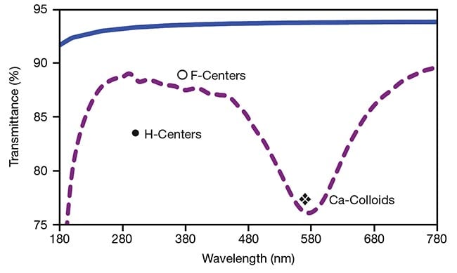
Figure 3. Spectral transmittance of enhanced
plasma-cleaned calcium fluoride (CaF2),
indicating absorptions associated with calcium
(Ca)-colloids, F-centers, and H-centers.
The Corning laser durable grade CaF2 crystal shows superior laser damage resistance in comparison to ArF laser-grade CaF2. Several generations of protective coatings for CaF2 (for example, PCCF and PCCFxi) further extend the lifetime of CaF2 laser optics.
High-energy x-ray coloration
High-energy x-ray exposure provides an effective means to simulate point defect formation in bulk and mobilization in comparison to the ArF laser-based accelerated lifetime damage test3. As a result, a high-energy x-ray coloration test was performed to compare the damage resistance between the earlier-generation material and the developed CaF2 material following laser plasma coloration.
X-rays are generated when accelerated electrons blast a metal target or anode. A heated tungsten filament produces electrons, which are accelerated in-vacuum by a high electric field in the range of 20 to 60 kV toward the metal anode. The corresponding electric current is in the range of 5 to 100 mA. The total intensity of the x-ray is proportional to the square of the accelerating voltage, the filament current, and the atomic number of the anode4.
The rhodium-anode x-ray tube, with an x-ray emission of 20 KeV, was used for the x-ray exposure experiment. The high-energy x-ray coloration may reveal buried sub-grain boundaries. Further, the purple coloration has a textured pattern that is clearly revealed over the magnetorheological finished wedge (Figure 4). In this case, this pattern may represent a collection of sub-grain boundaries interacting with the high-energy x-rays. Since CaF2 single crystals have sub-grains that have small angular misalignment, high dislocation density is expected to surround the sub-grains, forming sub-grain boundaries. The high dislocation density promotes purple coloration when exposed to high-energy x-rays.
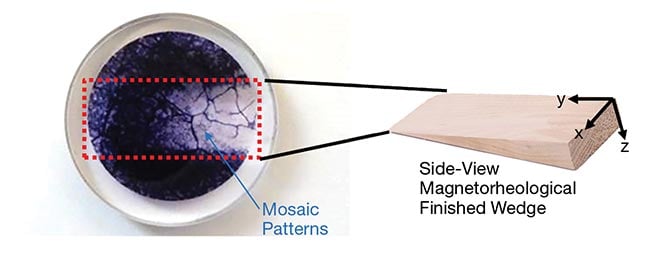
Figure 4. X-ray coloration of Φ1” calcium
fluoride (CaF2) after 12-h exposure followed
by a magnetorheological finished (MRFed)
wedge (left).
Also, in CaF2, dislocations are surrounding the sub-grain boundaries; these imperfections reduce the CaF2 bonding energy. The energetic radiation of the high-energy x-ray leads to the separation of fluorine atoms from the bonded CaF2 structure and the formation of fluorine vacancies. The aggregation of the fluorine vacancies forms high-density nanosized metallic Ca-colloids around the sub-grain boundaries. The Ca-colloids have a strong absorption of ~580 nm, leading to a purple appearance.
For surface quality assessment, three pieces of Φ1" CaF2 samples with different surface polish qualities were exposed to the high-energy x-ray for a period of 1.5 h (Figure 5). The intensity of the purple coloration is proportional to the subsurface damage on the CaF2 surfaces. In other words, the technique enables the visualization of the hidden subsurface damage layers.
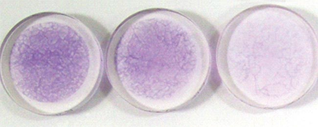
Figure 5. Three surface-polished Φ1” calcium
fluoride (CaF2) after 1.5-h x-ray test exposure.
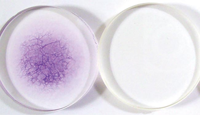
Figure 6. Deluxe polished Φ2” earlier-generation
material and laser durable grade
calcium fluoride (CaF2) after 3-h x-ray exposure.
For bulk crystal quality assessment, a pair of subsurface damage-free Φ2" earlier-generation material and laser durable grade CaF2 were exposed to the high-energy x-ray. The x-ray exposure time was doubled to 3 h for the bulk quality assessment.
Results
As shown in Figure 6, purple coloration does not appear on the subsurface damage-free laser durable grade CaF2. This result suggests that this material is more damage-resistant to the high-energy x-ray in comparison with the earlier-generation material.
Further, in acquiring the Raman spectra at ambient conditions, the pristine CaF2 (nonirradiated) showed a fundamental mode peaked at 320 cm−1 (Figure 7). The x-ray-irradiated sample, (or colored CaF2) has several additional broad peaks at 140 cm−1, 220 cm−1, 280 cm−1, and 430 cm−1. These peaks correspond to Ca-colloids5.
The high-energy x-ray coloration additionally appears to indicate that the developed material has superior crystal quality compared with the earlier-generation material, which is depicted in Figure 6.
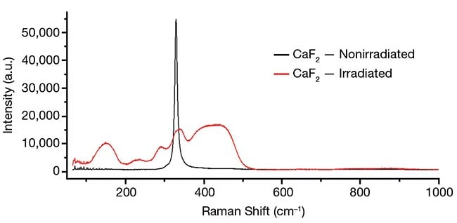
Figure 7. Raman spectra were acquired
following x-ray testing at ambient conditions.
A 100-mW laser at 532 nm was used to expose
the samples for 30 s. These spectra were
collected with five accumulations using a
quasi-backscattering geometry and micro
configuration with 100× magnification. The
pristine calcium fluoride (CaF2) (nonirradiated)
shows a fundamental mode peaked at 320 cm−1.
The high-energy x-ray coloration suggests that the developed laser durable grade CaF2 material has improved crystal structure in comparison with the earlier-generation material. This results in greater damage resistance to high-energy photons and indicates that it will be able to meet the demanding material specifications for laser optics.
References
1. J. Wang and G.P. Cox (November 2020). ArF laser-induced damage of calcium fluoride windows with protected antireflection coatings. Proc SPIE, Vol. 60, Article No. 3, Fairport, New York.
2. J. Wang et al. (March 2023). Surface and bulk damage resistance of calcium fluoride optics assessed by x-ray induced color centers. Proc SPIE, Vol. 12402, Article No. 8, San Francisco, California.
3. M. Babaeian et al. (December 2022). Hot-spot monitoring of ArF laser at HDC and high energy mode using low reflective beam splitter. Proc SPIE, Vol. 12300, Article No. 6, Rochester, New York.
4. P. Brouwer (2018), Theory of XRF, getting acquainted with the principles [booklet]. Almelo, Netherlands: Malvern Panalytical BV.
5. I. Alencar et al. (2016). Irradiation effects in CaF2 probed by Raman scattering. J Raman Spectrosc, Vol. 47, No. 8, pp. 978-983.