The growth trajectory of integrated photonics technologies necessitates a robust supply chain to support multiple materials platforms as well as design, manufacture, and test requirements.
ABDUL RAHIM, PHOTONDELTA, AND FAISAL KAMRAN, SONY EUROPE BV
The integration of photonic devices at the wafer scale has emerged as a transformative force, offering a reliable and scalable pathway to implement complex photonic functions cost-effectively on a chip. While integrated photonics has long been synonymous with optical communications, today’s landscape presents unprecedented challenges and opportunities — including those that fall outside the bounds of traditional optical telecommunications and data communications. As data volumes surge across growth sectors, the industry faces mounting pressure to deliver faster, more energy-efficient solutions and continuously improve the price-performance ratio.

Courtesy of iStock.com/ kynny.
The scale of this transformation is remarkable: Millions of transceivers now form the backbone of our digital infrastructure, providing high-speed optical connectivity across virtually every layer of the optical communications network. With data growth showing no signs of abating, the deployment of optical ports and integrated photonic transceivers continues to accelerate.
A recent European Conference on Optical Communication (ECOC, 2024) offered compelling insights into how the integrated photonics industry is adapting to meet the explosive traffic growth driven by AI and cloud services. The development of 100-GHz analog bandwidth electro-absorption modulated lasers, breakthroughs in thin-film lithium niobate (Mach-Zehnder) modulators, and the development of the first 200-GBd coherent driver modulator are among the latest solutions showcased by industry leaders. The availability of 800-Gbps transceivers and steady progress toward 1.6-Tbps capabilities further signal the industry’s relentless push forward. These advancements, coupled with innovations in pluggable transceiver form factors and the scaling feasibility serializer/deserializer (SERDES) to 400 Gbps, demonstrate the field’s upward trajectory. Similarly significant are the energy savings promised by co-packaged optics — though challenges persist in reliability, serviceability, and testability — as well as the potential energy efficiency gains enabled through linear-drive technology.
Call it ‘silicon’s second revolution’
What sets the current moment apart from those that have come before is the renewed appeal of integrated photonics for chip-scale optical connectivity. For the microelectronics sector, integrated photonics — and particularly silicon photonics — represents more than just another technology. Rather, it is an extension of silicon’s vast potential. This convergence enables the seamless integration of optoelectronic functionality with existing silicon capabilities, from logic to high-bandwidth memory and specialized features, to create powerful solutions for AI applications.
Vision to reality: The foundational years
The journey of integrated photonics traces back to a pivotal moment in 1969 when Stewart Miller shared his visionary perspective in the Bell System Technical Journal. Coinciding with Enrique Marcatili’s groundbreaking demonstration of an on-chip waveguide and directional coupler, Miller’s work — and the early days of the technology — were marked by a methodical quest to identify ideal material systems for photonic integration. Researchers meticulously evaluated various materials against a comprehensive set of criteria: their transparency window, potential for electronics integration, fabrication feasibility, and capability to perform both active and passive photonic functions.
This wave of exploration prompted intensive investigation of several promising material systems. Compound semiconductors such as indium phosphide (InP) and gallium arsenide, ferroelectrics such as lithium niobate, and various dielectrics underwent rigorous testing as researchers worked to demonstrate fundamental building blocks that would pave the way for more sophisticated photonic functions on-chip. A significant milestone emerged in 1975 with one of the first demonstrations of monolithic electronic-photonic integration.

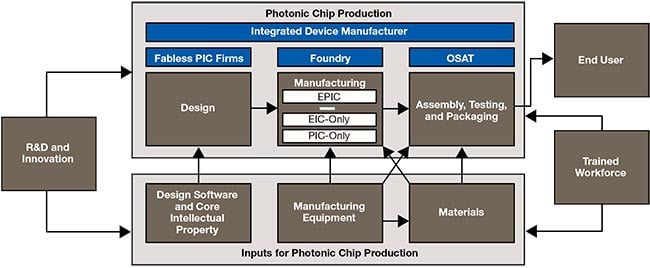
The photonic integrated circuits (PICs)
production framework illustrates the
interconnected ecosystem of design,
manufacturing, assembly, and end user
applications. Key stakeholders include fabless
PIC firms, integrated device manufacturers
(IDMs), foundries, and outsourced
semiconductor assembly and test (OSAT)
providers, supported by essential inputs
including materials, equipment, and workforce.
Original electronic integrated circuit (EIC)
foundries are engaging with silicon photonics
to increase wafer throughput. Some have
developed capabilities to integrate both into
electronic-photonic integrated circuits (EPICs).
See Acknowledgment 2. Courtesy of Center for Security and Emerging Technology (CSET).
By the late 1980s, the landscape of what would become today’s mainstream PIC platforms — InP and silicon photonics (both silicon-on-insulator (SOI) and silicon-nitride-on-insulator (SiN-on-insulator) — began to take shape. InP’s advanced position on the technology maturity curve culminated in a breakthrough: the first photonic integrated circuit (PIC) combining a laser and modulator in 1987. Another crucial development, the demonstration of a low-loss SiN waveguide, occurred in the same year and expanded the material possibilities for integrated photonics.
The rise of commercial platforms
The integrated photonics narrative took an interesting turn in 1985, when Richard Soref proposed the use of silicon as a material for integrated photonics through demonstrations of waveguides and switches on highly doped silicon substrates. Soref’s proposal was a major disruption: Compound semiconductors’ relatively mature position enabled rapid advancement in integrated functionalities, despite the fact that silicon was a newcomer to the realm of photonic integration.
In the dot-com era, photonic integration positioned itself as a cornerstone technology for telecommunications applications. InP PICs led the commercial charge, enabling the integration of tens of photonic components on a single chip. Meanwhile, SOI- and SiN-on-insulator-based silicon photonics, though still primarily in research phases, were making steady progress toward industry implications. This period culminated in the late 1990s with the emergence of early-iteration SOI PICs and Bookham Technology’s pioneering launch of the first silicon photonics product, in 1998.
A fascinating divergence in development paths would characterize the post-dot-com era. InP PICs continued their steady march forward, enhancing both building block performance and scaling densities. Vertically integrated InP PIC companies strengthened their market position, delivering increasingly sophisticated solutions tailored to telecommunications and data communications demands.


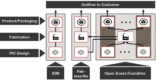
Access models for photonic integrated circuit
(PIC) manufacturing depict the transition from
vertically integrated device manufacturers
(IDMs) to more collaborative models such as
fabless/fab-lite and open-access foundries
(top). Fabless/fab-lite models either completely
outsource manufacturing or keep applicationspecific
in-house manufacturing while
outsourcing the rest. Open-access foundries
leverage economies of scale, standardization,
and ecosystem-wide innovations. Courtesy of IEEE. See Acknowledgment 1.
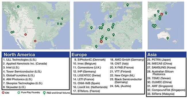
The silicon photonics foundry landscape.
Established and emerging silicon-on-insulator
(SOI) and silicon nitride (SiN) processes are
currently available with commercial foundries
and R&D centers (bottom). Courtesy of Abdul Rahim and Faisal Kamran.
At the same time, silicon photonics underwent its own transformation, marked by the pivot from thick SOI (with silicon guiding layers of a few micrometers) to thin SOI, featuring submicron silicon guiding layers. This shift enabled the development of silicon photonics building blocks on larger 200-mm substrates using established CMOS process tool sets. This transition to thin SOI enabled integrated device manufacturers (IDMs), fabless companies, research centers, and academic institutes to begin development of fundamental building blocks using a range of approaches. While thick SOI technologies maintain their relevance for R&D and certain commercial applications, this transition catalyzed widespread innovation in the technology space.
Democratization of photonic integration
Spurred by the advent of thin SOI, the efforts of engineers and manufacturers yielded impressive results, including low-loss passive devices, high-speed modulators, and advanced detectors. These developments laid the groundwork for significant commercial milestones, with Luxtera (since acquired by Cisco) launching commercial thin SOI silicon photonics products around 2007. Breakthrough products from Acacia Communications (Cisco) and Intel followed, and SiN PICs continued to evolve, though primarily within university laboratories.
Critically throughout this period, each material platform continued to strengthen its unique attributes and chart its own course. InP PICs distinguished themselves through fully monolithic integration of high-performance photonic functions spanning light generation and processing to detection. Silicon photonics on SOI substrates leveraged existing CMOS infrastructure and process tool sets, combining compact form factors with dense integration capabilities. The SiN variant carved its own niche by offering superior passive device performance and enabling applications beyond traditional telecommunications and data communications wavelength windows.
The open access revolution
The earliest commercially available PIC technologies were the exclusive domain of IDMs or a select few fabless companies engaged in joint development programs with IDMs (or with research foundries). Academic institutions played a crucial role in this landscape, with university and research center cleanrooms serving as incubators for groundbreaking demonstrations. These so-called hero demonstrations set benchmarks across the board. Among the most innovative are Bell Labs’ sophisticated 15 × 15 arrayed waveguide multiplexer on InP (1992); The National Centre for Scientific Research (CNRS)-University of Paris’ SOI-based ring modulator (1997); MIT’s ring resonator implementation (1999); Twente University’s SiN biosensor (1999); Zhejiang University’s silicon-based arrayed waveguide grating demonstration (2000); and Ghent University’s use of deep-UV lithography for SOI waveguides in collaboration with imec (2002).
In 2005, integrated photonics adopted the first of what would become many concepts from the established microelectronics industry — specifically the decoupling of design and technology offerings. The adoption of open-access multi-project wafer runs democratized access to PIC technologies developed by research institutes, making them available to any third-party designer at an affordable price. This democratization unfolded through several key initiatives: ePIXnet in 2004 (which later split into ePIXfab and JePPIX), followed by Opsis in 2012, and programs through the Agency for Science, Technology and Research (A*STAR’s) Institute of Microelectronics (IME), and Photonics Electronics Technology Research Association (PETRA). As the design community expanded, technology platforms began to standardize and mature, albeit in their own regional and technological silos. The initial development of passive and active building blocks has evolved into a sophisticated ecosystem.
The ecosystem emerges
Today’s integrated photonics landscape reflects this rich history of technological evolution and democratization. With a growing number of companies offering PICs-based solutions, a supply chain has begun to take shape. The convergence between integrated photonics and CMOS electronics supply chains has created opportunities and synergies, particularly as more materials, design, equipment, and packaging vendors from the CMOS microelectronics industry venture into integrated photonics technologies.
The evolution of integrated photonics from its conceptual beginnings in the Bell Labs era to this sophisticated ecosystem also tells a compelling story of technological persistence and innovation. The unprecedented demands of AI computation and the explosive growth in data center traffic have positioned integrated photonics as an enabler of communications as well as a fundamental solution to computing’s most pressing challenges. The semiconductor industry’s embrace of integrated photonics technologies, particularly as it moves toward a trillion-dollar milestone by 2030, marks a significant shift in the technology landscape.
Still, standardization must continue to provide access to mature routes, while democratization of integrated photonics technologies promises to accelerate innovation across multiple fronts. The industry’s delivery of higher speeds, lower power consumption, and improved cost structures will be crucial to address the computational bottleneck that stands between us and the next wave of AI advancement.
Elements of a supply chain
As integrated photonics matured from research-driven innovation into commercial adoption, its supply chain began to broadly mirror that of the microelectronics industry, especially in its blend of specialization with collaboration. The ecosystem now encompasses design/intellectual property (IP) houses, material suppliers, foundries, equipment vendors, and packaging providers. Each contributes to a cohesive pipeline that ensures the development of sophisticated PICs.

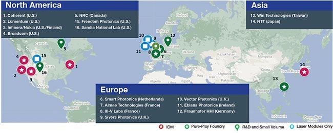
The present III-V PICs foundry landscape
shows a limited number of pure-play fabs to
balance a strong presence of integrated device
manufacturers (IDMs). Courtesy of Abdul Rahim and Faisal Kamran.
As it relates to PIC design, a modular dynamic, enveloping collaboration between photonic and electronic design houses, presented a great promise in aiding the optimization of circuit functionality. In the initial stages, PIC design relied on in-house tools tailored for specific projects. Today, advancements in electronic design automation (EDA) have ushered in sophisticated software solutions, enabling seamless PIC design. Major EDA vendors now integrate photonic design capabilities, facilitating the co-development of electronic and photonic circuits. Unified Electronic-Photonic Design Automation (EPDA) flows are emerging, too, enabling the optimization of electronic-photonic codesign and the optimization of building blocks through advanced physical-level simulation techniques. These include finite difference time domain, finite element method, and mode solving. As a result of photonic and electronic design houses collaborating in this way, comprehensive design stacks, incorporating pre-developed photonic IP blocks, continue to spread. This modular approach has broadly kickstarted innovation by enabling fabless companies and foundries to streamline development cycles.
In manufacturing, vertically integrated IDMs initially enjoyed dominance. This was particularly evident with InP technology. While IDMs remain key players, the ecosystem has evolved with the emergence of open-access foundries. European research institutes pioneered this shift, offering access to InP, SOI, and SiN platforms. Similar initiatives followed in the U.S. and Asia.
By 2014, commercial pure-play foundries had started to incorporate silicon photonics into their portfolios. And today, major microelectronics foundries offer open-access silicon photonics platforms. In SiN technology, the rise of boutique foundries for low-volume production, alongside larger players providing scalable 8-in. substrate processes, have spiked the prominence of this material platform. High-quality SiN processes often incorporate external partnerships to integrate active functions, enhancing performance and adaptability.
InP manufacturing predominantly relies on 2- to 4-in. wafers, but the growing demand for larger and more integrated PICs is driving a transition to 6-in. substrates. Meanwhile, silicon photonics benefits from mature 8-in. and 12-in. wafer platforms. Twelve-inch technologies offer superior uniformity and performance due to advanced process tool sets.
Design and simulation are not the only facets of the PICs ecosystem to borrow from the microelectronics industry. Integrated photonics heavily depends on the equipment and expertise of the microelectronics industry. Equipment vendors are tailoring existing tools to accommodate the unique requirements of PIC manufacturing, including the precise layering, etching, and lithography processes. As photonics continues to scale, these tailored solutions are ensuring the consistency and quality needed for high-volume production.
Packaging photonic chips presents a dynamic challenge; it requires solutions that address high-speed electronic interconnects, thermal management, and mechanical stability. The packaging landscape is diverse and fragmented, driven by the pressing need for cost-effective solutions. Recent innovations include the introduction of glass interposers, wafer-mounted interposers with detachable connectors, and advanced fiber attach techniques for specialized fiber arrays. Traditional gold box packaging has been a costly standard, and plastic packaging methods are now emerging, offering cost-effective alternatives without compromising functionality.
Electronic-photonic co-packaging is also gaining traction; large outsourced semiconductor assembly and test (OSAT) providers are investing in capabilities that bridge the two domains. Moonshot R&D projects aim to refine processes, such as wafer reconstruction and detachable optical connectors, while commercial entities are introducing assembly design kits (ADKs) to standardize packaging workflows. These ADKs enable designers to ensure compatibility between foundries and packaging houses, streamlining the production pipeline.
For its part, testing remains an integral — though underdeveloped — element of the integrated photonics supply chain. Unlike microelectronics, the industry lacks independent test houses, relying instead on in-house testing by fabs and packaging providers. Fortunately, wafer-level test tools now support the characterization of passive devices and low-to-high-speed active components. These tools are critical for maintaining quality control and ensuring that manufactured wafers meet stringent performance standards. The absence of independent test facilities highlights a potential area for growth as demand for PICs continues to rise.
Demand drivers and future needs
The supply chain for integrated photonics reflects the industry’s rapid evolution, mirroring the collaborative and innovation-driven nature of its microelectronics counterpart. From custom-built design tools to open-access foundries and modular packaging solutions, the ecosystem continues to mature, driven by advancements in materials, processes, and equipment. As demand surges across telecommunications, health care, and AI-driven applications, the supply chain must overcome fragmentation and scale its capabilities. The convergence of photonics and electronics ecosystems signals a promising future in which integration and standardization will unlock the full potential of PICs to meet the challenges of a data-centric world.
The integrated photonics supply chain is increasingly shaped by surging demand for high-performance transceivers, particularly in data centers. These devices form the backbone of global digital infrastructure and enable high-speed, low-latency data transfer essential for AI workloads, cloud services, and modern telecommunications. PICs play a critical role, delivering unprecedented energy efficiency and scalability. With projections of 3.2-Tbps transceivers by 2026 and the ongoing adoption of co-packaged optics, the reliance on integrated photonics for next-generation data center operations continues to expand.
Beyond data centers, integrated photonics is pivotal in automotive/autonomous vehicles (lidar), health care (biosensors and optical imaging), and quantum computing, where precision and miniaturization are paramount. These applications not only drive innovation in photonic manufacturing but also underscore the need for a robust, scalable supply chain.
The supply chain must adapt to new challenges and opportunities as applications diversify. Standardizing interfaces for the heterogeneous integration of materials is a pressing need. The integration of mainstream PIC technologies, such as silicon photonics and InP, into cohesive systems will be essential for optimizing performance and reducing costs. Ubiquitous access to unified electronic-photonic design flows is of equal importance. Enabling unified workflows would streamline the codesign of photonic and electronic components, fostering greater collaboration across the ecosystem and accelerating time-to-market for new solutions.
The growing demand for integrated photonics reinforces the need for a seamless connection between design, manufacturing, and packaging innovations. By addressing these future needs, the industry can meet the evolving requirements of high-speed computing, sensing, and communications.
Meet the authors
Abdul Rahim, Ph.D., serves as ecosystem manager at PhotonDelta, where he is developing an innovative integrated photonics ecosystem. He is dedicated to fostering collaboration among Dutch, European, and global stakeholders to drive advancements in the field; email: [email protected].
Faisal Kamran, Ph.D., serves as principal technology analyst at Sony. He is a leading photonics and business expert with extensive experience in technology evaluation, global collaboration, market analysis, sustainable business strategies, and mentoring startups; email: [email protected].
Acknowledgments
1. Image Attribution: The graphic is inspired by and modified from Proceedings of the IEEE Dec. 2018. Vol. 106, No. 12.
2. Image Attribution: The graphic is inspired by and modified from The Semiconductor Supply Chain: Assessing National Competitiveness. The Center for Security and Emerging Technology (CSET). Jan. 2021.