Martin Waeny, Awaiba CH SA
CMOS linear arrays allow the optical signal to be digitized directly on the chip, making the electronics design simpler, more cost-efficient and more robust.
CMOS image sensors were attractive initially because of their lower overall system costs, thanks to their higher integration level and the industry’s ability to place more and smaller pixels on a standard-size chip. Recently, the image quality of pixels produced by the latest-generation CMOS image sensor technologies has helped to infiltrate more niches where CCD technology still dominated the market.
One of these niche applications is spectrometry, where the image sensors are used in the form of linear arrays. New developments in CMOS-based photodiodes – and the combination of these with advanced readout architectures – enable higher-frequency readout and lower-input noise signal sampling. This is paving the way for CMOS-based line-scan sensors to allow novel spectroscopy applications or to improve existing spectrometer architectures.
CMOS linear arrays offer specific advantages over traditional CCD-based sensor architectures – most importantly, the option of digitizing the optical signal directly on the chip, making the electronics design simpler, more cost-efficient and more robust against noise pickup.
To understand the potential of CMOS-based digital linear diode arrays, it is convenient to examine first with more detail their generic architecture (Figure 1). The impinging radiation is absorbed and converted in an electric charge at the photodiode (shown in the figure as 1). The first-stage charge amplifier (2) converts the charge in a voltage signal. The conversion gain (and thereby the full well capacity) is defined by the size of the feedback capacitor. This permits the user to select the full well capacity independently of the photodiode size. In the second analog stage (3), the correlated double sampling is performed to separate the optical signal from low-frequency and reset noise. Finally, a sample-and-hold stage (4) allows capture of the signal synchronously from all photodiodes (global shutter). The on-chip AD converter (5) digitizes the signal and stores it in a per-pixel static random-access memory, or SRAM (6). The readout from the SRAM can be undertaken at high speed. Today, more and more low-voltage differential-signaling-based bit serial outputs are used to drive the off-chip data stream. This interface type allows easy, direct connection of the sensor to extended cabling solutions, and the sensor can be placed in a space-constrained sensor head or optical setup connected to the digital processing and control unit, only over a flexible circuit-board strip.

Figure 1. Functional block diagram of a digital linear photodiode array in CMOS technology. CDS = correlated double sampling; SRAM = static random-access memory. Courtesy of Awaiba.
A first and obvious benefit of CMOS linear arrays is the possibility of a substantially higher line rate, as compared with traditional linear diode arrays. In this architecture, all critical analog operations are performed on a per-diode or per-pixel level; those operations can thus be done with relatively low analog bandwidth – namely, the line rate. This reduces the random noise of the circuits, while the overall readout speed remains high-frequency. The readout of the pixels from the SRAM can be achieved at high speed and with low supply voltage, limiting both power consumption and noise generation. For example, Awaiba’s DR-4k-500 sensors offer a line rate of up to 46 kHz with a photodiode size of 7 × 500 μm. The more recent Orion series provides up to 85-kHz line rate at full resolution.
However, CMOS-based linear diode arrays offer advantages besides line rate and readout speed, allowing the sensor system to be optimized for specific spectrometric applications. One of these additional functionalities is known as Fowler sampling, or multiple nondestructive readout.
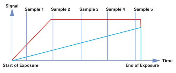
Figure 2. Principle of multiple nondestructive readouts. Courtesy of Awaiba.
The architecture in Figure 1 allows the pixel signal to be sampled multiple times during integration of the impinging signal. If the nature of the impinging signal is continuous, or if (as in the case of a pulsed source signal) its frequency is known, the signal resulting on the photodiode can be sampled several times, converted to digital and read out. The analog value will keep accumulating until reaching saturation during the multiple samples. Up and until saturation, the digital readings can be used to estimate the signal increase rate or the optical flux entering a certain photodiode. Noise can be reduced because of the multiple samples, approximately to a factor of the square root of the number of nonsaturated samples.
Once the signal of a certain pixel reaches the saturation level, the previously read signal from this pixel is used and scaled with its time stamp to extrapolate the final signal value of the pixel, if the sensor allows further integration without saturation. In this way, the total dynamic range of the sensor output can be increased by several orders of magnitude while maintaining a perfectly linear output representation. Figure 2 is a time diagram of the multiple nondestructive integration scheme, plotting the evolvement over time of two distinct pixel signals, one with high impinging radiation intensity (red) and one with low intensity (blue).
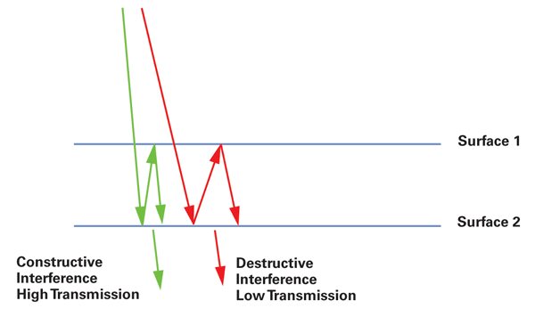
Figure 3. The principle of interference between two parallel surfaces leads to an etalon effect. Courtesy of Awaiba.
In the case of a low illumination signal (blue line), all samples (in Figure 2, all five samples) would be considered to estimate the slope of the pixel’s signal over the exposure time by a mean least-square linear fitting, or by Fowler sampling. Either of the two mathematical approaches permits reduction of read noise. However, for a signal with high illumination, only the samples up to the last nonsaturated signal are used. By combining just two samples, the dynamic range of the sensor can be extended by a factor defined by the longer exposure time divided by the shorter exposure time. When adding more intermediate samples, the extended dynamic range can be combined with noise reduction for the lower-intensity signals, thereby boosting the dynamic range even further, since the detection threshold is lower.
In spectroscopic applications, both a lower detection threshold and an extended dynamic range are much desired, because many spectral signatures require digitization of the high-intensity peaks, as well as the low-intensity side levels.
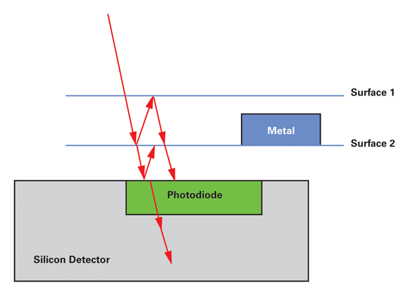
Figure 4. Source of etaloning in a front-side-illuminated sensor. Courtesy of Awaiba.
The etalon effect
A well-known complication when working with solid-state image sensors and narrow-bandwidth illumination is the etalon effect. The phenomenon occurs when monochromatic light impinges on a structure with two parallel surfaces that have at least some reflection and a distance less than the coherence length of the impinging light. The reflected party of the impinging illumination will then enter in constructive or destructive interference with the impinging light beam. Whether the interference is constructive or destructive depends on the wavelength and the angle at which the light impinges on the structure (Figure 3). The effect may be desirable and exploited when building a Bragg filter or an interferometer, but it is disturbing in spectrometry, as a small change in the impinging light wavelength or in the angle of the impinging light will strongly alter the detector’s response.
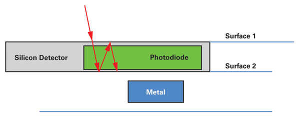
Figure 5. Source of etaloning in a back-side-illuminated sensor. Courtesy of Awaiba.
The etalon effect typically occurs when light can be reflected multiple times at the interface of a stack of transparent layers, but with a slightly different refractive index, because it is usually found on top of the photodiode in an integrated semiconductor detector with front-side illumination (Figure 4).
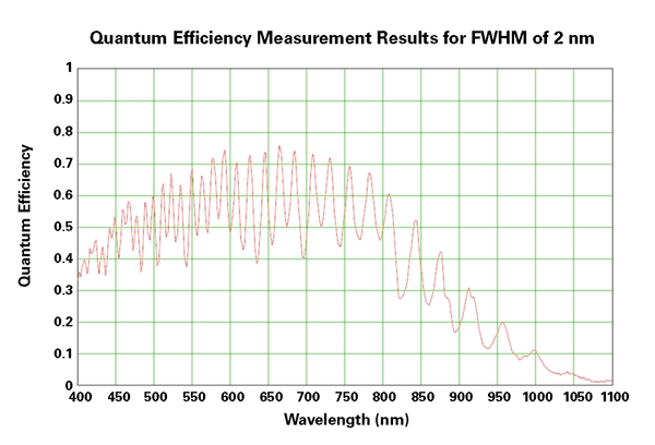
Figure 6. The spectral dependence of quantum efficiency of a front-side-illuminated line-scan image sensor showing a strong etalon effect. FWHM = full width half maximum. Courtesy of VTT Institute Finland.
The effect is also known from thin back-side-illuminated detectors, where the light generates interference by reflection between the entrance surface and the silicon-to-electronics interface at the sensor front side (Figure 5). The near-infrared part of the impinging radiation will survive one or several round-trips between the two interfaces in a back-side-illuminated sensor particularly easily, as the total thickness is typically only a few microns.
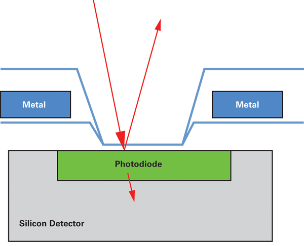
Figure 7. The principle of a front-side-illuminated etalon-free photodiode. Courtesy of Awaiba.
The etalon effect leads to a spectral response that is very uneven and shows, at a constant angle, a strong wavelength-dependent oscillation of the spectral response. If the illumination on such a sensor is close to monochromatic, the response can vary significantly as a function of very small variations in the angle of the impinging light, or as a function of small variations caused by manufacturing
tolerances in the thickness of the reflecting layers. Figure 6 shows the spectral quantum efficiency of a sensor suffering from the etalon effect when illuminated with narrow-bandwidth light impinging with a constant and narrow incident angle.
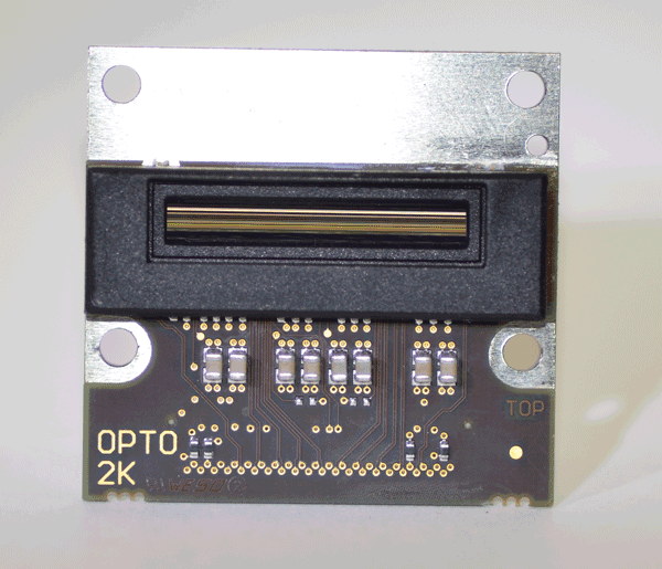
Figure 8. The Orion digital line-scan sensor has a protective cap to prevent bond-wire damage in the glass-free version. Courtesy of Awaiba.
A special manufacturing process for fine-pitch linear image sensors from Awaiba allows the use of a front-side-illuminated sensor. These devices allow the user to work with several hundred microns of silicon thickness, eliminating the risk of round-trip interference between the front- and back-side silicon interface. To avoid multiple reflections on the stack of intermetal dielectric and chip-passivation materials, a window was opened on each photodiode, removing all layers above the photodiode and depositing an antireflection coating only
a few nanometers thick on top of it; Figure 7 provides a cross-section sketch of the structure.
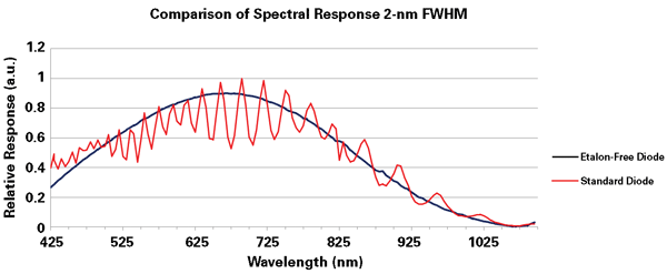
Figure 9. The spectral response of the 1K Orion sensor with the etalon-free diode, compared with a standard CMOS photodiode. Courtesy of Awaiba.
Designed for spectroscopy applications, the Orion family has a configurable read-out chain that allows for a line rate of up to 85 kHz at full resolution over bit-serial low-voltage differential signaling output. The sensors integrate the novel etalon-free photodiode and are available in a package with or without a glass lid, to avoid any risk of multiple reflections or unwanted absorption. The bond wires are protected from mechanical damage by a specially designed cover cap (Figure 8). The etalon-free photodiode removes any type of etalon effect over the full spectral range.
Meet the author
Martin Waeny is the CEO of Awaiba Holding SA in Yverdon-les-Bains, Switzerland; email: [email protected].