
High-Speed Segmented MEMS for Large- Aperture Optical Switching
The Teledyne MEMS foundry in Edmonton, Alberta, has been manufacturing light valves using a variety of approaches since 1994. This article discusses its surface-micromachined, megahertz-capable approach.
By Glen Fitzpatrick
The term “light valve” refers to a device that can be used to control many individual beams of light from a single illumination source. As an enabling component for a range of both consumer and highly specialized systems, the evolution of these devices is characterized by the availability of multiple configurations on the market. Today, with multiple designs and products commercially available, end users can select their preferred device type for their system.
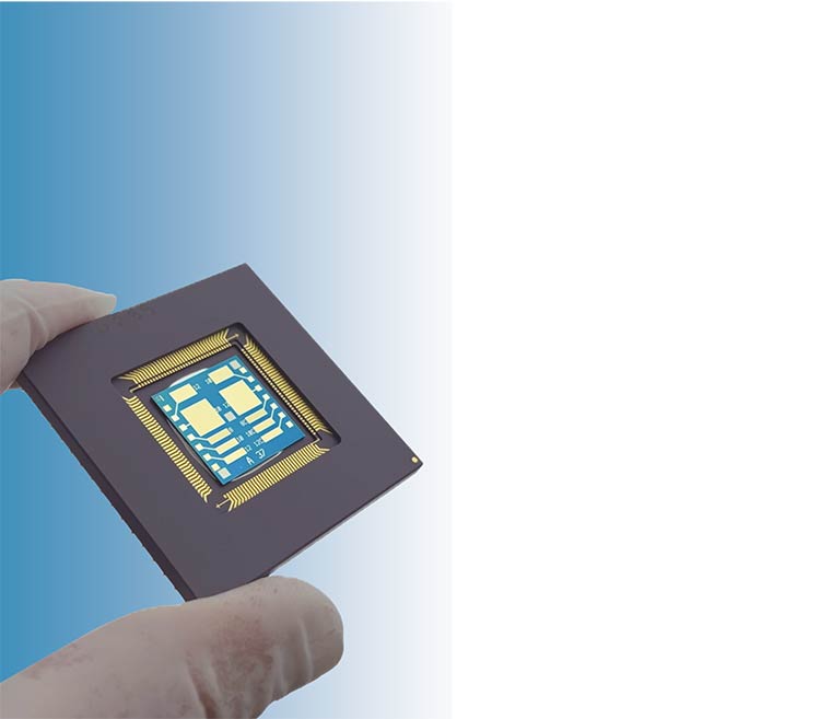
Ten fabricated test devices are shown in-package. Courtesy of Teledyne MEMS.
Because it is a broad term, “light valve” has been used throughout its history to describe liquid crystal on silicon (LCOS) as well as the digital micromirror device (DMD) developed by Texas Instruments. Both architectures are examples of 2D arrays. Silicon Light Machines’ grating light valve (GLV) technology, meanwhile, is the best-known example of a linear array light valve.
These designs demand a high channel count, which is a requirement that has led industry to fabricate each of these approaches on a driver CMOS-based backbone for signal management, with the microelectromechanical system (MEMS) fabrication subsequently fabricated on the surface of the electronics. Although liquid crystal devices are often described as solid-state, because their operation depends on the physical movement of molecules in a viscous medium, it is best to consider such devices mechanical for the purposes of this article.
The widespread recognizability of the GLV holds true today, as these devices remain among the most widely used solutions for linear-array light modulation in display, imaging, and printing applications. GLVs use alternating grating subelements that move 1/4 wavelength electrostatically to either reflect (zero order) or form a diffraction grating for each pixel at hundreds of kilohertz.
Silicon light valve
Teledyne MEMS’ silicon light valve (SLV) leverages a similar approach to the GLV — a linear array of electrostatically driven switching elements. However, the MEMS portion is built solely on the silicon substrate, with addressing performed on the surface. Thousands of connections are made through individual address
lines to packaging leads. So, while more packaging requirements are imposed, the design approach offers distinct advantages — both optically as well as mechanically.
While this technology could be incorporated into CMOS flows, the multielement design raises the possibility of enabling single-channel applications. The MEMS process flow can use a wide range of materials and processes unsupported in/by CMOS. Further, the design is aperture-agnostic and retains a higher cyclic frequency than other approaches, with a high fill factor that provides mirror-like reflectivity.
In this way, the developed system represents a reconceptualization of a design — proven in high-channel-count, high-resolution, and high-speed IR imaging systems — into a simple, high-speed, large-aperture optical switch.
Single-channel modulators
Multiple methods for single-channel
intensity switching are already established. Compared with conventional mechanical methods, both acousto-optic (AO) and electro-optic (EO) modulation devices are favored solutions for systems and applications that require greater speed. In terms of MEMS solutions, few commercial approaches offer the necessary speed to qualify as high-speed modulators, and in general, all inertial systems decrease in speed with increasing size scale.
With AO and EO methods, however,
increasing the aperture incurs higher costs for the high-purity crystals and their coating and bonding processes. The MEMS approach, in contrast, scales cost less dramatically due to the wafer scale efficiency. Acoustic propagation constraints slow response times in AO crystals as aperture requirements increase. Meanwhile, high-voltage requirements across the crystal aperture as it increases limit the repetition rates of EO devices.
The underlying approach to an AO device is to couple an acoustic signal to a crystal, where the acoustic waves then interact with the optical beam. The transmitted beam is then diffracted at an angle as the radio frequency (RF) power is applied to the transducer, reaching a maximum relative intensity dictated by the physics of the system, which is described as the diffraction efficiency. The RF frequency value, modulator size, and power set the grating structure and, therefore, the diffracted beam angle. The relationship with the RF power requirements is constrained by the crystal’s coupling coefficient. Tellurium dioxide, for example, has a high coupling coefficient and is often used. Other materials offer their own advantages in a variety of optical applications.
Today, major suppliers offer options with apertures up to 15 mm, though devices in the 0.3- to 3-mm range are the most widely used. This is largely due to switching speed limitations beyond this range, which result from the transit time of the acoustic signal across the aperture. For context, a 5-mm SLV can offer the same bandwidth as a 0.3-mm tellurium dioxide modulator and could still likely extend to both larger and faster options.
For some applications, AO approaches fail to offer fast enough switching times. EO modulators — particularly transverse EO designs, where an electric field is placed on each side of the crystal to change polarization within the crystal — offer a higher-speed, though more
expensive, alternative. By referencing static polarizers, applying the appropriate voltage to cancel the polarization, known as Vπ or the half-wave voltage, allows light to pass.
The switching speed of most EO systems is in the nanosecond range for free-space optics. As the aperture increases, the voltage required to switch generally becomes larger, which can increase the time between switching, or the repetition rate. However, this also this depends on the drivers and the crystal material.
The high switching speed (nanoseconds) yet low repetition rate (kilohertz) seems counterintuitive, and the SLV could potentially achieve nanosecond switching speeds. Repetition rate is not limited in the SLV’s mechanical system; it would simply switch at whatever speed is desired for the application within the range at which the resonance speed is maximum.
Amplitude modulation: MEMS approach
In the progression, or reimagination, of SLV technology, using the device as a single large-intensity or optical-power modulator creates an opportunity to use the simplicity of a mechanical design at higher switching speeds than other mechanical methods have been able to achieve. While still a member of the light valve family, using the SLV as a single large-intensity or optical-power modulator opens opportunities for free-space optics, using pluralities of the device structure cross section (Figure 1). When the elements are actuated, they tilt, and the energy is redirected from the normal angle1.
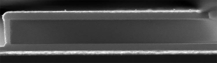
Figure 1. A scanning electron microscopy image of the cross section of a single 10-μm-wide tilting element. Courtesy of Teledyne MEMS.
Numerous iterations of test device geometries were fabricated to demonstrate the viability of this approach, showing that it can deliver a large-aperture,
mechanically based device that achieves the speed of a small individual element with a single input voltage. Figure 2 shows confocal microscope images of
actuating 12-μm-wide elements. Test
device lengths were increased incrementally to validate the theory, and multimillimeter devices have proved to still function at a high resonant speed. Still, the practical limit for aperture remains unknown.
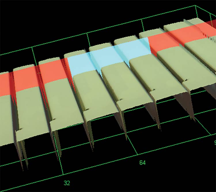
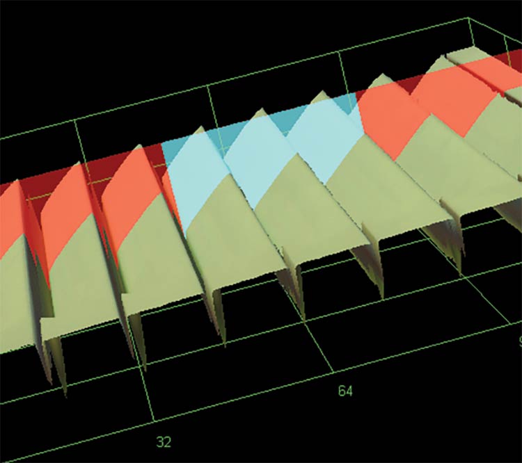
Figure 2. A confocal microscope image of undeflected elements (top). A confocal microscope image of all elements in the field of view being actuated by a single voltage input (bottom). Courtesy of Teledyne MEMS.
The limited section of the tilting
element at the boundary condition of edge support in models and measurements is a transitional shape for ~60 μm; however, the central section maintains the shape through actuation and is independent of length. Test outputs ultimately show a 2.6-MHz switching speed for a group of 333- × 5-mm-long tilting mirrors operated with a single input voltage.
The practical limit of the speed relationship is not fully known, and the company has, to date, limited the study to the practical speed requirements for imaging applications. Still, adjustments to the design and materials could easily influence this metric to further increase switching speed.
A viable alternative
While much of Teledyne MEMS’ study proved to be useful for multichannel device characterization and development, it demonstrated that all elements could
be made identically so that the group characteristics manifested synchronously upon actuation. From this, the possibility has emerged to use a single-channel voltage input using elements with a characteristic width that is speed-invariant with aperture. Optical models and measurements of even a single tilting, mirror-like element at the width scale of ~10 × λ
switch as a single channel, and an array simply acts as a larger switch. This behavior has been tested from visible to far-IR wavelengths.
This explanation of the mechanism of operation can now be used to understand how this may be used as a simple planar device to modulate the intensity of a large aperture at speeds beyond what conventional mechanical solutions can offer.
Of course, the demonstration must be placed in the appropriate context. As mentioned, compared with AO and EO modulators, few MEMS-based
approaches are currently considered fast enough to qualify as “high-speed” modulators. However, both AO and EO systems often use aperture-reducing optical design strategies. A MEMS solution based on the described test protocol promises to
be performance-agnostic with respect to the aperture size. It can also be designed to specification through relatively straightforward MEMS mask layout and fabrication adjustments (See Tables 1 and 2).
Also, in this context, the solution and approach described pertains to larger (>300-μm)-aperture free-space optics using high-bandwidth designs. Numerous
AO and EO options for a variety of applications exist in the marketplace. And various strategies exist to trade off different characteristics.
The utility and potential of such a MEMS-based solution are rooted fundamentally in existing SLV performance
capabilities. By demonstrating megahertz-range switching speeds independent of aperture size, SLVs offer the manufacturability and robustness of traditional
MEMS-based optical modulation systems, with an agility and configurability factor that is compelling for optical designers.
Meet the author
Glen Fitzpatrick was the founding manager of the University of Alberta Sensors and Actuators lab in 1987. The lab evolved into Micralyne, which is now the Edmonton, Alberta, division of Teledyne MEMS; email: glen.fitzpatrick@teledyne.com.
Reference
1. N. Pilossof (Sept. 30, 2014). Asymmetrical deformable diffractive grating modulator. U.S. Patent No. 8848278. U.S. Patent and Trademark Office.
/Buyers-Guide/Teledyne-MEMS/c3384