Photonics HandbookFeatures
High-Resolution Image Sensors Set New Standards in Machine Vision
CMOS image sensors have achieved >200-MP resolution for advanced applications. Integration of this technology must overcome challenges such as optical performance, frame rate, and complex power management.
By Prashant Mehta
The transformation of digital imaging in recent years has had a profound impact on its applications in machine vision and even the life sciences. From the nascent days of CMOS image sensors capturing 10,000 pixels (0.01 MP) with pixel sizes of 20 to 30 µm, imaging has entered an era of high-resolution image sensors packing >200 million pixels (>200 MP), with pixel sizes now shrinking to <1 µm. This incredible progression in resolution is not just a technical marvel — it is reshaping the landscape of digital image processing and continually pushing the boundaries of what is possible. This evolution has opened a range of new applications and is now used in fields such as industrial inspection, medical imaging, and autonomous systems.
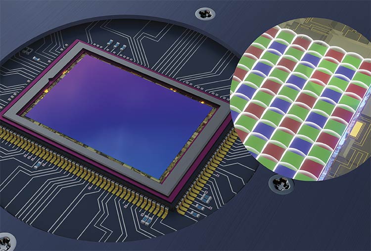
An enlarged digital camera backside-illuminated matrix and a full view of a modern digital photography sensor. Courtesy of iStock.com/atdigit.
Technical hurdles
The smallest pixels currently available on image sensors are ~0.56 µm. Although this could enable high resolution in a small sensor footprint, such a small pixel size comes with various challenges. The technical challenges that have arisen from pixel and sensor miniaturization include the resulting effects on quantum efficiency, full-well capacity, signal and noise behavior, and dynamic range, to name a few. And, with the increase in resolution, it is challenging to transfer all the captured image data to the attached processor in a timely fashion to continue to support frame rate.
In initial CMOS sensor designs — namely, front-side illumination — pixels have areas designated for absorbing light, called light-sensitive photodiodes or photosites. Outside this area, the space is devoted to electronic circuits, which are necessary for pixel operations. This area does not collect photons; hence, front-side illumination pixels collect less light than theoretically possible for a given pixel area due to the reduction in their light-absorbing surface area. The electronics of the individual pixels consume valuable space and thus reduce the light-collecting “active” area. This can be measured by the pixel fill factor, or the ratio of light-sensitive and light-insensitive areas of the pixel. As the pixel size decreases, it is important to increase the pixel fill factor and maximize the light-facing area used to collect photons.
The smaller pixels, in general, also collect fewer photons due to their size. This reduces the sensitivity and quantum efficiency, or QE, which is calculated by dividing the number of electrons generated by the number of incident photons and multiplying by 100%. In other words, this is the value that indicates how effectively a single pixel converts the collected light into a detectable charge that is used to generate the image data. In essence, fewer photons are collected, resulting in fewer generated electrons, which are essential for producing image data.
The lower QE is compounded by limited charge storage capacities (full-well capacity) due to smaller pixel structures. This affects the dynamic range in imaging because smaller structures are also more susceptible to thermal influences that generate dark currents, which results in increased image noise.
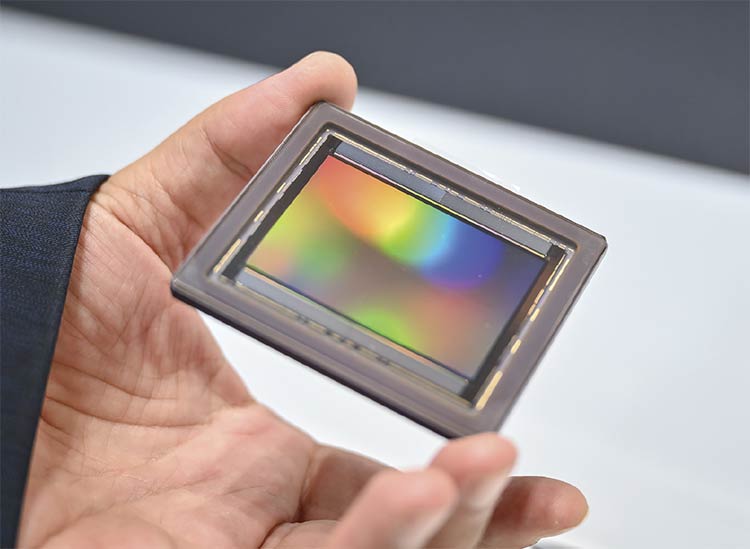
The Sony IMX811, a high-resolution image sensor. Courtesy of FRAMOS.
As pixel sizes shrink, light diffraction becomes a significant factor that leads to crosstalk. This occurs when a photon incident on one pixel is detected in an adjacent pixel. This misdirection of light has several negative consequences for image quality.
There are two main types of crosstalk:
• Optical crosstalk occurs when photons themselves cross pixel boundaries before being converted into an electrical signal.
• Electronic crosstalk occurs when photogenerated electrons diffuse into neighboring pixels after conversion.
Regardless of the type, crosstalk introduces inaccuracies into the final image. A particularly noticeable effect is color distortion. Modern image sensors use a Bayer matrix, an arrangement of color filters, to capture color information. When light diffuses into the neighboring pixel, color is inaccurately reproduced. This light diffusion also reduces image sharpness, a phenomenon often measured by a lowered modulation transfer function (MTF), which describes the transfer of contrast from an object to an image.
Essentially, crosstalk occurs when a photon that enters one pixel is “read” by a neighboring pixel, resulting in blurry images with compromised color accuracy.
Manufacturers’ solutions
Semiconductor manufacturers such as Sony have made great strides in recent years in reducing the undesirable effects of ever-smaller pixel structures. One of the most significant innovations in image sensors in recent decades
has been the introduction of back-side illumination pixels. Using this technology, the sensor is manufactured in such a way that the light from the rear of the silicon chip strikes the light-sensitive photodiodes directly.

More than a rule of thumb — more pixels require a more complex power supply arrangement. The final row reflects the incr+easing number of power supplies as the resolution increases. Courtesy of FRAMOS.
In conventional sensors, such as front-side illumination, the metal wiring is located between the light source and the photodiode, which not only reduces the light-sensitive area as described previously, but also creates shading effects, thereby reducing the effective aperture. The back-side illumination process eliminates this shading, allowing the entire surface of the pixel area to be used for light collection or any application that uses a CMOS sensor. This leads to higher pixel fill factor, increasing the sensitivity and quantum efficiency, and enables the individual pixels on the sensor to be smaller without compromising image quality.
The less severe problem of crosstalk can be effectively mitigated by the creation of a “trench” between pixels. This technique, known as trench isolation or deep trench isolation, has been employed in CMOS sensors since around 2010 and involves etching trenches into the silicon substrate and filling them with a dielectric, such as silicon oxide. This structure reduces crosstalk, thereby preserving modulation transfer function and preventing unwanted color mixing.
Sensor integration
The integration of high-resolution image sensors is also more complex than that of lower-resolution sensors. More pixels also mean more circuits. The readout circuits must process larger amounts of data. A larger number of pixels and faster readout increase power consumption and power management requirements. This results in more complex power circuits that operate with more voltage states. Even slight fluctuations in the power supply have a direct effect on image quality, which can lead to noise artifacts. Image noise can severely compromise the accuracy of automated inspection, such as measurement and recognition tasks, for example. When large amounts of data are generated, more power is consumed. This generates heat, which is always problematic for image sensors — after all, a user would want low-noise images, which can only be obtained if the sensor can operate undisturbed by excessive thermal influences. The power circuit must therefore work dynamically and efficiently. This is directly reflected in the operating voltages of high-resolution sensors.
Thermal management
Because the sensor size and the associated circuit board size typically increase with the number of pixels, thermal stability becomes an issue for target applications, because more surface area also means more heat. This problem can be solved with adaptive circuit board designs — for example, by integrating holes into the circuit board to enable more effective heat circulation and dissipation. Heat sinks are also used. However, this can affect mechanical stability, so a more stable design must be ensured.
Sensor size and lenses
C-mount and M12 lenses are widely used in industry — in closed-circuit television and machine vision cameras, and in embedded cameras, respectively. However, the typical sensor sizes of high-resolution image sensors are larger on average and thus affect the size of the associated lenses. The IMX811, for example, is a 4.1-in. type with a diagonal of 64.84 mm. It requires a larger-format lens (M48 or higher) to completely cover the large image circle resulting from such a large sensor active area. The number of suitable lenses is still rather low but will certainly increase as resolutions >200 MP become more common. As the size of the sensor increases, the tilt of the sensor and lens grows, affecting the image focus. All these issues will probably be addressed by updating measurement systems in the future. However, existing processes and methods can be transferred and must be revised in tandem with lens mount definitions.
Suitable data interfaces
Another notable challenge lies in transferring and processing the vast amounts of data produced by high-
resolution sensors. Higher-resolution sensors produce much more data than typical 2-MP or 5-MP sensors.
One could look at the IMX811 (19200 × 12800 pixels, 245.76 MP) to illustrate the enormous amounts of data produced: With a 16-bit readout bit-depth and 5.3 fps, the RAW data amounts to an enormous 2.6 GB/s. By comparison, a 1080p video with 12 bits and 60 fps would use 0.12 Gbps. Even with the use of techniques such as pixel binning, subsampling, and (theoretical) compression (not supported by the IMX811 sensor), the data volumes are still extremely high. So, if a user wants to operate the sensor at maximum frame rate with the highest bit-depth, the imaging system will require a high-bandwidth data transfer interface.
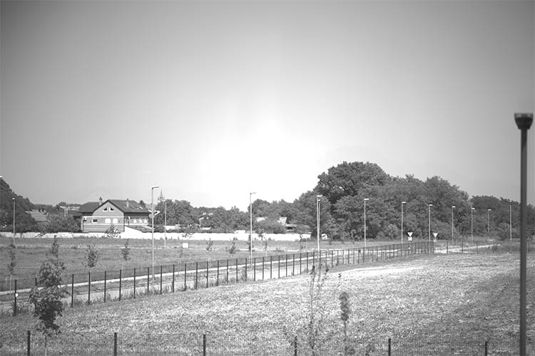
A test image produced by the Sony IMX811 image sensor. Courtesy of Sony.
In addition to the widely used MIPI CSI-2 (Mobile Industry Processor Interface Camera Serial Interface 2), the SLVS-EC (Scalable Low Voltage Signaling with Embedded Clock) interface is designed to meet these high data transfer requirements. Two parameters are particularly relevant here: the transmission capacity per lane and the number of lanes that are implemented. With MIPI CSI-2 (version 3.0), which is mainly used for mobile phones, for example, the figure is 9 Gbps with four lanes. SLVS-EC (version 3.1), which is now available on the latest Sony sensors for machine vision, supports transmission speeds up to 12.5 Gbps, with specifications supporting eight- and even 16-lane configurations.
The receiving processor board capable of handling such large amounts of data must also be designed to receive, process, and retransmit high data volumes — for example, from cameras using popular machine vision interfaces such as CoaXPress, CameraLink, or
N-BaseT GigE. For reference, the IMX811 sensor employs the SLVS-EC interface, outputs at 9.2 Gbps per lane, and uses up to eight lanes to transfer the large amount of captured information.
A potential solution to such high data transfer may be to process images on the sensor itself and transfer smaller data sets of processed results. Such AI-based approaches — for example, with Sony’s IMX500 sensor — aim to reduce data volumes. This is urgently needed because, even though the IMX500 is not a high-resolution sensor per se, the idea behind this technology addresses a problem regarding the massive amounts of data that must be transferred off-chip and processed, which all high-resolution image sensors require. The sensor can process the data on-chip, eliminating the need to transfer it to a back-end processor for analysis.
Market demand for high-res sensors
Of course, system integrators and camera manufacturers want the best possible image sensor for their system, and that often means that high-resolution sensors are in demand. One could argue that more pixels are better, but a high-resolution sensor may be unnecessary for many applications and would produce massive amounts of data that must be transferred and processed, as explained above. This would drive up the cost of the processing hardware.
For example, if the application involves checking the fill level of liquids in bottles, an image sensor with a low resolution would be sufficient, which in turn would require less complex hardware. The additional resolution would not improve the application’s performance and would increase costs unnecessarily.
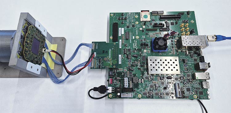

A test setup for a high-resolution image sensor. Courtesy of Framos.
For many applications, ranging from robotics to logistics, a resolution in the range of 2 to 5 MP or 5 to 8 MP may be sufficient. Additionally, if relative motion occurs between the camera and the object being imaged, it may be preferable to choose a global shutter sensor. A global shutter sensor does not produce the distortion artifacts associated with a rolling shutter and often offers options for higher frame rates, accurate triggering, and even the ability to reduce exposure times to extremely small values. Nowadays, global shutter sensors commonly offer recording speeds >100 fps, enabling high throughput. However, certain application areas benefit from the use of such high-resolution image sensors. Some of them are outlined below.
Factory automation
In industrial automation, high-resolution image sensors are used to inspect large and complex electronics components, such as flat panel displays, high-density interconnect printed circuit boards, and solar cell modules. With a high-resolution sensor, an entire inspection object can be captured in a single image. The high resolution of the captured image will enable the verification and inspection tasks associated with it. The processing software ensures that all the expected electronic components and features are present. Even smaller defects, such as microcracks, dust inclusions, or minute structural deviations, can be detected.
With a lower-resolution sensor, multiple image captures may be required, and it may also require image stitching. The high-resolution sensors enable higher throughput and seamless quality control without mechanical movement or multiple positioning of the test object. This significantly increases production throughput while raising defect detection to a new level of precision. Stitching introduces its own errors, but since high-resolution sensors perform single-shot imaging, no such issues arise. The high image resolution also enables simultaneous measurement of component dimensions and the verification of assembly or manufacturing tolerances, which provides decisive advantages compared with traditional sensors in terms of efficiency, speed, and reliability, especially in series production and automated production processes.
Life sciences
High-resolution sensors also play a crucial role in biotechnological and pharmaceutical research, especially in automated high-throughput microscopy. When biological samples such as cell cultures or tissue sections are analyzed, it requires the processing of many sequential slides. Since cellular changes often occur in the submicrometer range, sensors must offer not only high resolution, but also excellent noise suppression, high dynamic range, and accurate color reproduction.
Modern sensors >100 MP enabled large areas of a slide to be captured with a single image without losing details at the cellular level. This accelerates data collection and increases the accuracy of algorithmic evaluation by AI-based diagnostic systems. This combination of area coverage and depth of detail is particularly indispensable in drug development, for example, to comprehensively and reproducibly analyze cell responses to potential drugs over a period of time.
Quality control
Finally, another highly specialized application area is industrial quality control, particularly in semiconductor manufacturing and the inspection of microstructured surfaces. In this use case, ultrahigh-resolution sensors are used — for example, to inspect the entire surface of 300-mm wafers and identify defects in the submicrometer range. These sensors must not only offer enormous depth of detail but also be able to operate at high speeds to keep pace with industrial cycle times. They are part of automated inspection systems used to detect defects such as scratches, particles, lithography errors, and structural deviations.
Similar technology is also used in the flat panel display industry to detect pixel errors, contrast irregularities, and color deviations in high-resolution OLED and liquid crystal display panels at an early stage. The use of such image sensors contributes significantly to quality assurance and reduces scrap and production costs through early detection of process deviations.
In all these applications, it is clear that image sensors exceeding the 200-MP limit are not an end in themselves from a technical standpoint, but a technological necessity — either for imaging large areas without the loss of information or for reliably capturing microscopically small structures. The technical challenge lies not only in the sensor architecture itself but also in its integration into optical systems, in data processing, and in ensuring high image quality in real-world conditions.
Future outlook
Image sensors in the triple-digit megapixel range are enabling important industrial applications. The technical hurdles involved in their development pose significant challenges. However, resourceful engineers and researchers have so far managed to keep pace and deliver their promise of ever higher-resolution sensors. In the future, the gigapixel barrier is projected to be broken.
Meet the author
Prashant Mehta has more than 20 years of experience in engineering, technical sales, and product development. He has a master’s degree in imaging science and is a technical imaging expert at FRAMOS US Inc., with extensive expertise in image sensors, machine vision systems, and embedded vision platforms. Throughout his career, Mehta has been instrumental in fostering strategic partnerships with
industry leaders and driving innovation in applications ranging from autonomous driving to industrial robotics; email: p.mehta@framos.com.
Published: September 2025