
Five Drivers Will Shape the Future of High-Power Laser Diode Technologies
As high-powered laser diode technology enters its next phase of growth, the drivers shaping the technology’s success are opening opportunities for device designers to innovate.
By Mark Crowley and Prabhu Thiagarajan
High-power laser diode (HPLD) technologies are driving innovation across a range of applications, from industrial — in materials processing and aerospace and defense — to those in the domains of medical, sensing and detecting, and communications. HPLD technologies are also critical enablers of fundamental scientific research, such as particle accelerator systems and laser fusion-based energy production.
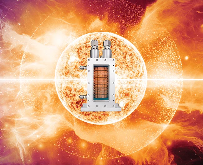
Courtesy of Leonardo.
In most of these application scenarios, the laser diode is typically a variation of the broad-area, edge-emitting HPLD and functions as the initial photon source for the given system. These devices are used to pump an external gain material, such as an optical fiber or a solid-state gain material. The external gain material is used as a brightness converter to mitigate
the inherently divergent beams of edge-emitting HPLDs. Despite the need for this additional component, the gallium arsenide-based, broad-area, edge-emitting HPLD remains the world’s most efficient light source.
As applications emerge and existing applications evolve, advancements in emitter epitaxy, novel device concepts, improved packaging concepts, and cooling technologies are among the factors that promise to shape the progress of HPLD technologies. In conjunction, these areas of progress are already pushing the boundaries of device performance.
Fundamentally, however, five drivers
— namely, higher optical powers and efficiency, higher brightness, smaller size and weight, improved reliability, and lower cost — hold the greatest influence over the future of HPLDs. With device developers actively working to improve technologies for each of these considerations, it is unclear which HPLD technology will dominate in the years ahead.
Toward next-generation systems
The electrically pumped area of broad-area, edge-emitting HPLD single emitters typically ranges from tens to hundreds
of micrometers in width by a few millimeters in cavity length. Broad-area HPLD bars are collections of many single emitters arranged adjacent to one another in
a single semiconductor chip with a width of 1 cm and thickness of 120 µm. The single emitters are optically isolated from each other using physically etched trenches or ion implantation.
The process of producing broad-area HPLDs begins with the deposition of epitaxial layers on a 3- to 6-in.-diameter substrate. This action is performed via III-V growth techniques such as metal-organic chemical vapor deposition and/or molecular beam epitaxy. The vertically grown stack of semiconductor layers includes an active layer sandwiched between waveguide and cladding layers, which serve to guide the light field and transport electrical energy to the active region where it is converted to photons. Wafers are processed through a series of steps based on ultraviolet lithography to define the individual emitters and their metal contacts. Bars are then cleaved,
and their facets are passivated and subsequently coated with dielectric layers to form a rear facet of high reflectance and an output facet of lower reflectance.
Advancements in several important device characteristics over the last decade have enabled significant improvements to performance, particularly in optical power (Figure 1). For example, facet passivation technology gains have increased the damage threshold of the facet to withstand ever-higher photon densities. As a result, kilowatt-class diodes have
become available in volume, and the power envelope continues to reach new heights (Figures 1 and 2).
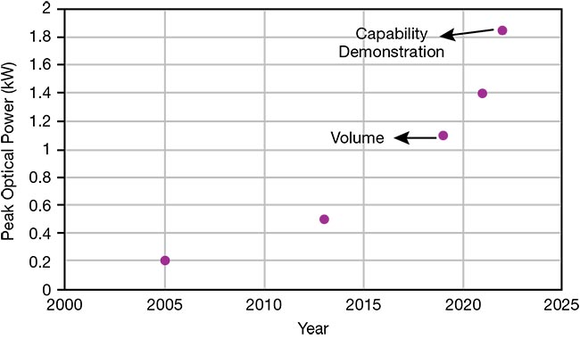
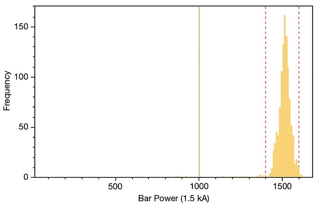
Figure 1. Leonardo high-peak-power laser diodes at wavelengths spanning 750 to 1600 nm, producing peak output powers >1200 W/bar. The evolution of peak optical power for a single p-n junction under quasi-continuous-wave operation at 25 °C ambient temperature (top). Production distribution for Leonardo kilowatt-class diode bars (~1000, 3-in. wafers) (bottom). The quasi-continuous-wave value is 250 µs and 20 Hz. Courtesy of Leonardo.
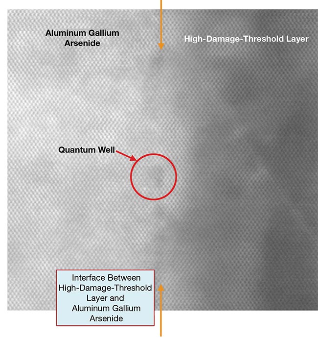
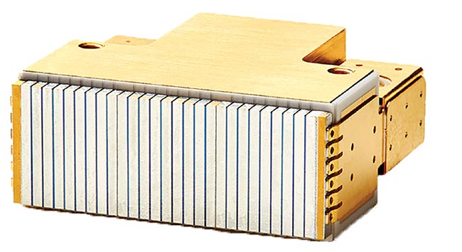
Figure 2. Advancements in facet passivation technology have increased the damage threshold of the facet to withstand ever-higher photon densities in laser diode architectures (top). Aluminum gallium arsenide (AlGaAs) is the semiconductor material in the laser structure. The crystalline layer adjacent to the AlGaAs layer is the high-damage-threshold (HDT) facet protection layer (bottom). Courtesy of Leonardo.
Meanwhile, the introduction of new epitaxial designs that minimize electrical and optical losses has charted a path for steady improvements in electrical-to-optical efficiencies. Single-bar peak efficiencies of >70% have been reported for broad-area HPLDs with values approaching >60% for kilowatt-class bars (Figure 1)1.
These advancements have direct ties
to laser diode improvement across the spectrum of powers and broad applications. They also set the stage for the
parameters of higher optical powers, higher efficiency, higher brightness, smaller size and weight, improved reliability, and lower cost to define forthcoming growth in HPLDs. As technology advances, there is an ongoing drive to lower size, weight, power consumption, and cost — critical to next-generation laser systems.
Yet, despite these advancements, the brightness of broad-area HPLDs remains a challenge, and these lasers are typically used to pump another optically active gain medium such as fiber lasers or solid-state lasers. Additionally, to fully realize the potential of these high-power devices, it is imperative that cooling technologies keep pace with advancements in both diode technology and material quality.
Surface-emitting architectures
An alternative approach to laser system architectures involves eliminating the brightness converter and using diodes
directly in the final application. Such direct diode solutions can be far more compact, efficient, and cost-effective.
Photonic-crystal surface-emitting lasers (PCSELs) are one example of this emerging technology trend. These sources have the potential to achieve many benefits — namely, high-brightness coherent lasing — compared with more traditional edge-emitting lasers as well as more
established types of surface-emitting lasers.
A typical PCSEL structure consists of a photonic crystal layer composed of a 2D in-plane periodic refractive-index distribution, an active layer for light amplification, waveguiding layers, and electrodes for current injection (Figure 3). The periodicity of the air holes in the photonic crystal is designed to create a 2D standing-wave resonance over a large area, culminating in lasing oscillation
accompanied by coherent surface emission.
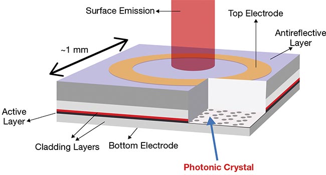
Figure 3. A schematic of a photonic-crystal surface-emitting laser (PCSEL) structure. Adapted from Yoshida et al. See Reference 4. Courtesy of Leonardo.
A 3-mm-diameter PCSEL can operate at power levels up to 1 kW under pulsed conditions. Continuous-wave lasing at
50 W has also been demonstrated, with an extremely narrow divergence of <0.5°2. However, challenges remain concerning the manufacturability and efficiency of these specialized diodes. That being said, the direct diode concept can, in principle, be achieved by any of the various HPLD technologies. It is widely regarded as the holy grail of laser diode technology.
A more widely adopted surface-emitting source, the vertical-cavity surface-emitting laser (VCSEL), can achieve emission of a single spatial optical mode. Additionally, due to its use of monolithic distributed Bragg reflectors (DBRs), VCSELs can also achieve a significant degree of spectral brightness. VCSEL arrays can also be arranged on a single chip, establishing a critical advantage and enabling burgeoning application opportunities for these lasers.
However, VCSEL brightness is less than that of a PCSEL, and their efficiency falls short of edge-emitting lasers. Edge-emitting, tapered, single-mode ridge waveguide lasers have emerged as a technology that can achieve high brightness that rivals current PCSEL technology3. Such devices are based on a flared chip architecture, which can deliver high output power(s) with nearly diffraction-limited beam quality.
In Figure 4, light generation occurs in the rear section of the architecture, which has the geometry of a single-spatial-mode ridge waveguide that is combined with a DBR. This section produces both a single-spatial and spectral-mode optical output, which serves as the input for the subsequent power amplifier section. Then, the power amplifier allows the emission from the rear section to expand through diffraction. This occurs as it propagates toward the exit facet to the right of Figure 4.
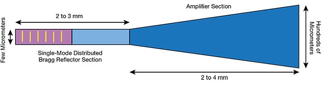
Figure 4. A schematic of a single-spatial and spectral-mode high-power, edge-emitting laser diode. Courtesy of Leonardo.
This design approach enables a much lower peak optical intensity within the cavity and on the exit facet compared with a traditional single-mode diode. Therefore, the output power and reliability of the device is enhanced. Additionally, the thermal resistance of the device is significantly reduced, enabling much higher optical power extraction compared with the regular single-mode device.
Even though these device architectures achieve excellent brightness, their overall efficiency still falls short when compared to a broad-area HPLD.
Road map and opportunity
The demand for, and competition among, different HPLD technologies is apparent, spurred by clearly defined technology drivers. Looking ahead, substantial investment is required to improve each of these drivers in parallel.
Achieving this goal requires both
continued innovation and a focus on large-scale applications. These drivers
also have eventual limitations; for example, recombination processes that compete with stimulated emission, the finite conductance of semiconductor
materials, and the turn-on voltage of a diode are each fundamental limitations
to higher optical power. Unless a paradigm shift in technology occurs, improvements in power and efficiency will eventually reach a point of diminishing returns.
Nevertheless, current applications will push the cost envelope further as volumes and markets mature. Improvements in manufacturability — which have often characterized and stimulated growth in the electronics industry in the past — along with the implementation of AI-based automated defect screening, are anticipated to increase yields, enhance quality, and improve cost efficiency. And as noted, additional technological developments to improve performance, such as novel chip designs and/or improved thermal packaging, are reducing the price per watt.
The current expectation that these factors will converge to define the future of HPLD technologies does not diminish the progress that was achieved during the last two decades. During this time, R&D and industry have pioneered a tremendous evolution in laser diode technologies. Yet, while different technologies offer distinct sets of strengths, combining all features into a single uber-device has continued to elude the diode community.
Today, opportunities continue to develop in emerging and existing markets that demand higher and higher levels of
performance. As new, more demanding, and higher-volume applications arise,
the drivers will remain relevant and push the frontiers of what is possible.
Meet the authors
Mark Crowley, Ph.D., is the director of device technology at Leonardo Electronics US Inc. He has more than 20 years of fundamental research, product development, and technology management experience in the field of semiconductor devices; email: mark.crowley@leonardo.us.
Prabhu Thiagarajan, Ph.D., is senior vice president at Leonardo Electronics US Inc., where he manages the Laser Solutions business line. He has more than 30 years of experience in the laser industry and has authored more than 50 publications; email: prabhu.thiagarajan@leonardo.us.
Acknowledgments
The authors wish to thank Leonardo’s Laurel Lunsford and Robert Walker for their contributions to this article and assistance in completing the text.
References
1. P. Crump et al. (2025). Power and efficiency scaling of GaAs-based edge-emitting high-power diode lasers. IEEE J Sel Top Quant Electron, Vol. 31, No. 2, pp. (99):1-12.
2. S. Noda et al. (2024). Photonic-crystal surface-emitting lasers. Nature Reviews, Vol. 1, pp. 802-814.
3. A. Müller et al. (2017). 10.5 W central lobe output power obtained with an efficient 1030 nm DBR tapered diode laser. Proc IEEE High Power Diode Lasers and Systems Conference, pp. 61-62, Coventry, England.
4. M. Yoshida et al. (2021). Photonic-crystal lasers with high-quality narrow-divergence symmetric beams and their application
to LiDAR. J Phys Photonics. Vol. 3,
No. 022006, pp. 1-15.
/Buyers-Guide/Leonardo-Electronics-US-Inc/c8243