Exponential growth in data communication is driving bandwidth demands in hyperscale data centers.
SUNIL PRIYADARSHI, INTEL CORPORATION
Courtesy of iStock.com/kynny.
The relentless expansion of data communication, propelled by advancements in artificial intelligence (AI) and machine learning workloads, as well as cloud computing, cloud storage, AR/VR, video on demand, 5G technology, the Internet of Things, and autonomous vehicles, demands a substantial increase in bandwidth. Hyperscale data centers are under continuous pressure to enhance and augment their network capacity. This is achieved through hardware upgrades, including more advanced switches, routers, and servers, which offer higher bandwidth via increased port speeds and higher port counts relative to previous generations.
In parallel, the optical interconnects that link these network devices must also scale their bandwidth capabilities. Over the years, this scaling has been accomplished through advancements in lane speeds, modulation techniques, and the number of lanes (Figure 1).
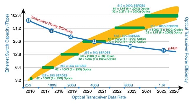
Figure 1. The evolution of Ethernet switch bandwidth
and optical pluggable transceiver bandwidth
based on vendor disclosures and public
announcements. SERDES: serializer/
deserializer. Courtesy of Intel Corporation.
Pluggable optical transceiver modules are essential components in data communication systems, widely used as optical interconnects at the termination of fiber optic links. These modules perform the critical function of converting electrical signals into optical signals, and vice versa. They are designed to insert into networking equipment, such as switches, routers, and servers, in which they interface with the fiber optic cabling that interconnects hyperscale data centers and enterprise networks.
These transceiver modules are engineered for hot swapping, which means that the transceivers can insert or be removed from their network ports without interrupting operation or powering down the network equipment. This allows for easy maintenance, upgrades, and installation.
These pluggable optical transceivers conform to standards defined by multi-source agreements (MSAs), such as Small Form Factor Pluggable (SFP), Quad SFP (QSFP), QSFP-Double Density (QSFP-DD), Octal SFP (OSFP), and Common Management Interface Specification (CMIS). These standards specify the connector pinouts, dimensions of the transceiver(s), power consumption, and communication protocols with the host board. A single optical transceiver definition under an MSA can support a multitude of transceiver types, which may vary in the number of lanes, optical wavelengths, signal formats, and link reach.
This standardized approach affords network architects the flexibility to select from a wide range of optical transceivers without the need to alter the underlying electrical switch design(s) (Figure 2). For example, a variety of optical transceivers are supported within the QSFP-DD form factor, including 400GBASE-SR8, 400GBASE-DR4, 400GBASE-FR4, 400GBASE-LR4, and 400GBASE-ZR4. These products differ in their connector types, carrier wavelengths, modulation formats, and maximum transmission distances.
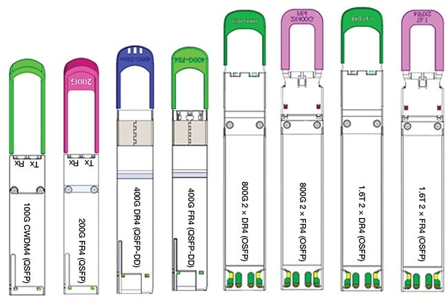
Figure 2. An example of different form factor
and data-rate pluggable optical transceivers. Courtesy of Intel Corporation.
And, while MSAs ensure interoperability among devices, they also provide network architects the freedom to choose product architectures that meet specific requirements and enable cost reductions. Amid the current surge of data and telecom demands, this variance in architectures is particularly relevant for high-volume deployments in hyperscale data centers.
Pluggable transceiver design
As the bandwidth of optical transceiver modules increases, technical challenges are emerging for members of the engineering community tasked with the design of pluggable optical transceiver modules. This complex design process requires the integration of multiple technological disciplines. Challenges relate to high-speed operation, an increased number of host channels, power constraints, thermal management requirements, and electrical specifications. Electrical, mechanical, optical, and firmware engineering must collaborate precisely to deliver the required electro-optical performance.
A pluggable optical transceiver module architecture consists of several critical components: a laser light source capable of high-speed modulation, a modulator driver, a photodetector, a transimpedance amplifier (TIA), clock and data recovery units (CDRs), digital signal processors ((DSPs) or gearboxes), a microcontroller, and voltage regulators that power various power rails. These components are essential for the module’s operation (Figure 3).
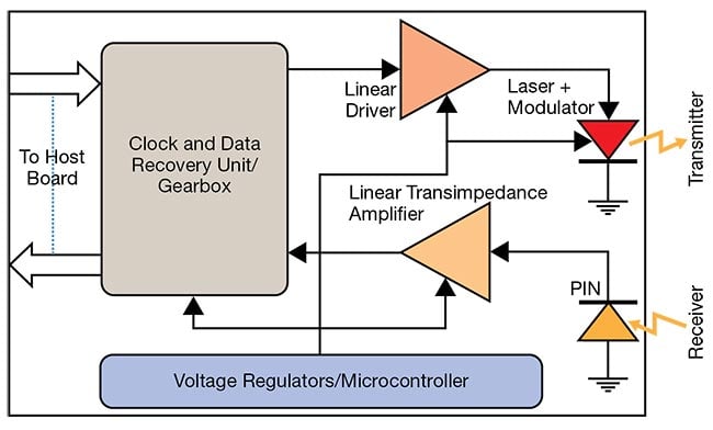
Figure 3. A diagram of an optical transceiver. Courtesy of Intel Corporation.
Table 1.
Transmit (Tx) Specification for 800GBASE-2 × DR4
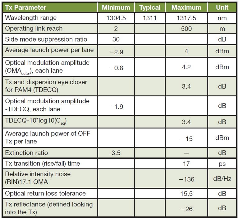
In a pluggable optical transceiver, the input electrical signal received from the host board is first processed using a retimer. The purpose of a retimer mechanism is to eliminate jitter that has been introduced by the host’s serializer/deserializer (SERDES) and to correct any other signal impairments that may be introduced while the signal is transmitted from the host board to the module PCB. For example, in an OSFP-800GBASE-2 × DR4 transceiver, eight lanes of 53.125 Gbaud PAM4 signals are retimed to remove jitter. The retimed and amplified signals are then used to modulate the intensity of the output laser. A variety of optical modulators, such as directly modulated lasers (DMLs) and electro-absorption modulated lasers (EMLs), can be implemented to achieve this modulation. The modulated light is then coupled into the optical fiber using lenses.
Silicon photonics-based Mach-Zehnder and ring modulators can also be used. Mach-Zehnder modulators (MZMs) and ring modulators both use interferometric structures to translate refractive index changes into optical intensity modulations. Both are key components in silicon photonics-based transceivers, offering distinct advantages and trade-offs, including between one another. MZMs are favored for their high extinction ratios, higher linearity, thermal stability, and ease of fabrication, though they suffer from high power consumption and a larger footprint. In contrast, ring modulators offer small footprints, favorable bandwidth, and low optical loss, though they have high thermal sensitivity, which means that they require accurate temperature control to achieve optimal performance. They also have a limited operational optical bandwidth. Fabrication techniques, such as p-n junction-based MZMs, are straightforward but less modulation-efficient compared with carrier injection and accumulation methods. Power consumption in these devices is primarily determined by the voltage required to achieve a phase shift of π radians. Ultimately, the choice between MZMs and ring modulators depends on specific application requirements influencing performance, thermal stability, power consumption, and fabrication complexity.
On the receiver side of a pluggable optical transceiver, if the incoming light signal contains more than one wavelength, it is first demultiplexed. In operation a photodetector then converts the optical signal into an electrical current waveform. This current is subsequently converted into a voltage waveform by a TIA. The voltage waveform is then processed through a retimer to mitigate any impairments introduced by the fiber, such as dispersion or jitter. If necessary, the signal is passed through a gearbox to adjust the data rate before it is transmitted back to the host board.
Optical transceiver specifications
Optical transceivers must adhere to all relevant specifications to ensure interoperability among devices produced by different vendors. IEEE 802.3 task forces typically define the electrical and optical specifications without specifying form factors. The IEEE specifications encompass the optical link budget, transmit (Tx) and receive (Rx) specifications at the physical layer, and the media access control at the data link layer.
Complementarily, MSA groups (such as OSFP) specify form factor-related requirements, including power supply voltage, connector pinout, mechanical dimensions, optical connector definitions, and the host control interface. For instance, the 800GBASE-2 × DR4 is a single-mode fiber-based optical transceiver that features eight parallel Tx/Rx optical lanes with a center carrier wavelength of 1310 nm. Each lane is required to operate at 100 Gbps and support a minimum link reach of 500 m. Tables 1 and 2 list the specifications for the Tx and Rx as defined in IEEE 802.3ck-2022 and IEEE P802.3df, respectively.
In addition to optical, electrical, mechanical, and reliability specifications, optical transceiver modules are also required to meet environmental and safety compliance standards. And, they must be designed with manufacture and test in mind — concepts known as design for manufacture (DFM) and design for test (DFT) optimize manufacturing throughput and yield with the ultimate aim to minimize production costs. Given the diversity of optical transceivers available on the market, each produced by different vendors with their own distinct technological approaches, there is no one-size-fits-all design methodology or workflow that is applicable to all types of optical transceivers or vendors.
Discrete vs. silicon photonics
Silicon photonics technology has gained significant traction within hyperscale data centers in recent years, and it is increasingly prevalent as the demand for larger volumes of pluggable optical modules increases within these facilities. Traditionally, the manufacture of optical transceivers has involved the use of discrete optical components. This process entails the manual assembly of free space DMLs, EMLs, photodetectors, isolators, optical multiplexers and demultiplexers, lenses, and fiber termination connectors. These components are typically integrated into gold-box or ceramic substrate assemblies. Figure 4 shows an example of such a Tx subassembly, for a 400GBASE-DR4 transceiver using EMLs.
As shown in Figure 4, the necessity for multiple active and passive optical alignments during manufacturing that characterizes this subassembly process makes it quite labor-intensive and costly. In the case of a 400GBASE-DR4 Tx subassembly, for example, EMLs mounted on a substrate must first undergo a burn-in process and subsequent testing to eliminate any of these components that fail. Following this, four discrete EML substrates are individually mounted onto a ceramic substrate, which serves as an optical bench. Four discrete lenses are then positioned on the bench, followed by four pieces of two-stage isolators, and finally, four discrete glass ferrules with polarization lenses are aligned, resulting in a total of 16 discrete component alignments.
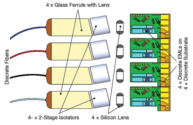
Figure 4. A 400GBASE-DR4 transmitter (Tx)
subassembly with discrete components (right).
EMLs: electro-absorption modulated lasers. Courtesy of Intel Corporation.
A 400GBASE-FR4 transceiver requires the incorporation of an additional discrete optical multiplexer. The complexity of this manufacture increases significantly in doubling (or quadrupling) for 800G and 1.6T 2 × DR4/FR4 Tx subassemblies when using discrete components.
Owing to the complexity of these design requirements, industry-led innovations, including those pioneered at Intel, have targeted simplifications — as well as performance improvements — for the manufacture of optical transceivers. For example, Figure 5 shows an 800G 2 × FR4 Tx PIC with dimensions of 5.77 × 10.72 mm. This Tx PIC, based on Intel silicon photonics technology, integrates 8× DFB lasers (2 × 4 coarse wave division multiplexing (CWDM)) 4 λs, 8× MZMs, 16× quadrature bias heater/monitor photo detector, 8× variable optical attenuator, 2× temperatures diodes, 8× MZM biasing terminations, 2× edge inverted taper optical out, and 2× quad optical multiplexers, both optical active and passive components, totaling more than 50-plus individual components.
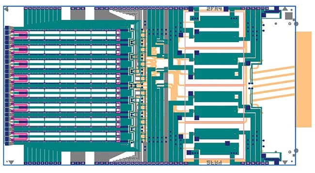
Figure 5. An 800GBASE-2 × FR4 transmitter
(Tx) photonic integrated circuit. Courtesy of Intel Corporation.
Consequently, this technology eliminates the laborious assembly process involved with discrete fabrications. In fact, the PIC in this system necessitates only a single active alignment to couple it with the fiber assembly unit (Figure 5). Intel’s silicon photonics technology enables the integration of the complete Tx and Rx optical systems within a PIC, which can significantly reduce the number of assembly steps, manufacturing time, and production costs.
Heterogeneous integration
There are additional necessities to consider beyond design and development, and many are located downstream from fabrication. Wafer integration — targeting the development of integrated hybrid lasers — as well as delivery to customers are two additional requirements that Intel is meeting. The company has shipped its integrated solution in mass volume, and more than 8 million PICs and more than 32 million on-chip lasers have been deployed in the field. A critical advantage involves the use of a process that enables monolithic integration — in this case, of indium phosphide (InP) and germanium onto silicon wafers. This process is used to create integrated lasers, as well as optical amplifiers and photodetectors, which offer integrated laser sources inside the PIC. This integration eliminates the need for external laser sources, semiconductor optical amplifiers (SOAs), and/or photodetectors, which represents a requirement that can add design complexity and increase costs.
As shown in Figure 6, InP epitaxial-material chiplets are placed onto a 300-mm silicon-on-insulator (SOI) wafer. Then, the lasers are patterned and created at wafer level, including the inscription of gratings into the silicon material. This process enables the fabrication of highly complex chips that integrate multiple lasers with different wavelengths, along with numerous other passive and active components.
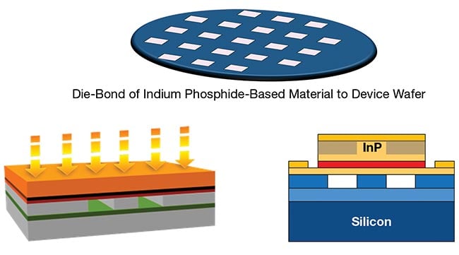
Figure 6. An integrated laser/semiconductor
optical amplifier (SOA) at wafer scale.
InP: indium phosphide. Courtesy of Intel Corporation.
Integrating optical gain directly onto the photonics chip offers a significant advantage in simplicity, performance, and cost. Consider that chip-scale laser integration using conventional discrete lasers is often plagued by reliability issues. Using DFB lasers, the absence of exposed facets, and the elimination of mechanical stress from grinding, polishing, and singulation — all of which are common in the production of discrete lasers — characterize the integration designs. Figure 7 displays the laser characteristics over temperature and bias current as well as the flexibility of incorporating multiple CWDM wavelengths within a single PIC.
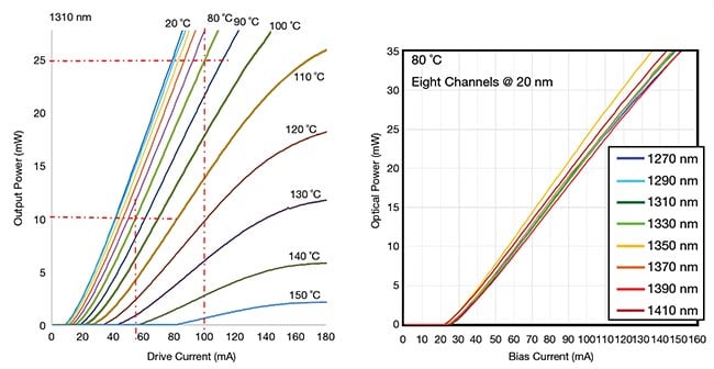
Figure 7. Integrated laser characteristics over
temperature (left) and bias current
(right), as well as the flexibility of
incorporating multiple coarse wavelength
division multiplexing (CWDM) wavelengths
within a single photonic integrated circuit. Courtesy of Intel Corporation.
These integration approaches aim to streamline manufacturing efficiency and automation by reducing discrete components and manual processes. As a result, the technology serves to increase overall factory output. Additionally, wafer-level burn-in and testing allow for extensive automation and high production rates, making the mass production and adoption of leading-edge optical transceivers more attainable. Silicon photonics also enhances product yield through consistent and reliable component performance, due to the precision of lithography and wafer etching techniques. Early detection and correction of design-related issues are possible through statistical modeling and simulations, which predict transceiver performance before manufacturing.
Further, economies of scale are realized as the up-front investment in chip design is amortized over increasing production volumes, enabling efficient, high-volume production. As optical modules proliferate in data centers, the benefits of silicon photonics will be amplified, making high-speed optics more widely available in the market.
The path to 1.6T and 3.2T
Transitioning from 800G to 1.6T optical modules as AI workloads in data centers escalate will effectively double the bandwidth capacity per 1 rack unit (RU) without requiring modifications to the existing infrastructure. With the current use of 800G pluggable modules, a 2RU rack is necessary to support a 51.2T switching capacity across 64 ports.
On the other hand, the adoption of 1.6T pluggable modules would allow the same 51.2T capacity to be achieved within a single 1RU rack using only 32 ports. Furthermore, the shift toward 200G/lane optical links in data centers sets the stage for 1.6T and 3.2T optical module solutions with 200G/lane serial electrical interfaces. This is essential for supporting next-generation 102.4T switches and expansive AI clusters, such as the NVIDIA GB200. Also, the direct 1:1 mapping between electrical and optical I/O speeds enabled by 200G/lane signaling from the application-specific integrated circuit (ASIC) eliminates the need for gearboxes or multiplexers, and thereby streamlining the implementation of 1.6T or 3.2T optical modules.
Figure 8 shows a 1.6T 2 × FR4 PIC. This architecture is similar to that of the 800G 2 × FR4, but this solution features eight high-speed MZMs operating at 200 Gbps, simplifying the design of 1.6T optical modules on an OSFP platform. A 3.2T capacity could be achieved using two such PICs on an OSFP-extended density (OSFP-XD) platform. Figure 9 depicts the implementation of a 1.6T optical module in an OSFP platform using Intel’s PICs and integrated electronic circuits. Intel’s 1.6T optical module solution, for example, enhances bandwidth density by 2×, optimizing the space in data centers.
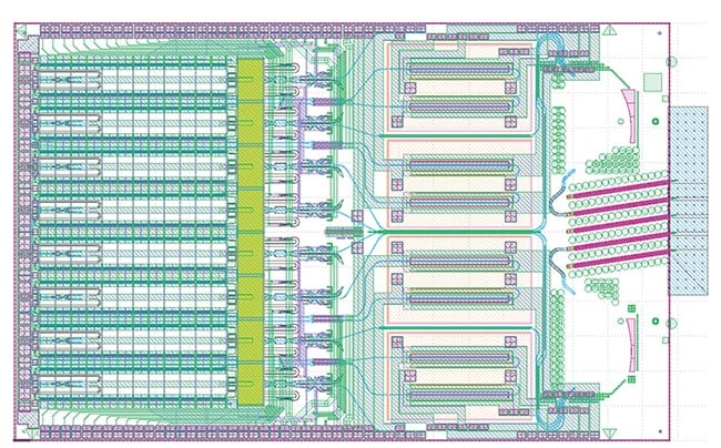
Figure 8. A 1.6TBASE-DR8 photonic integrated
circuit. Courtesy of Intel Corporation.
Table 2.
Receiver (Rx) Specification for 800GBASE-2 × DR4
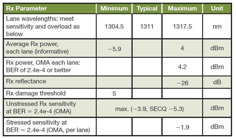
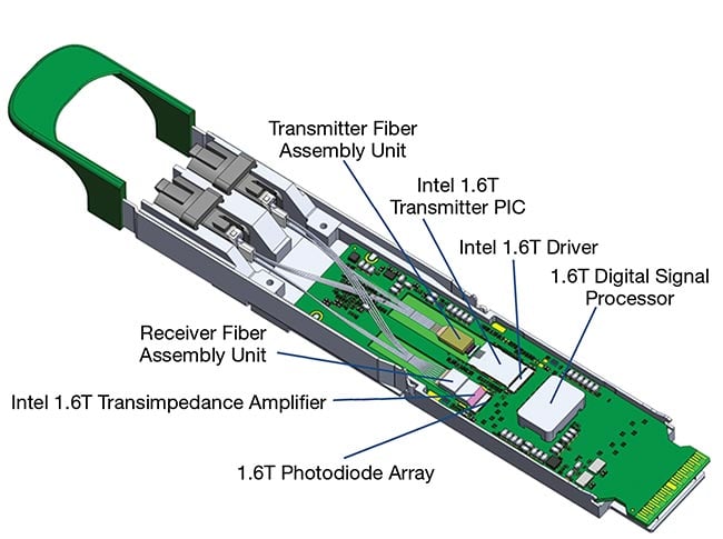
Figure 9. An architecture of a 1.6TBASE-DR8
module, using an Intel photonic integrated
circuit. Courtesy of Intel Corporation.
Co-packaging and compute interconnect
In current iterations of switch systems, signal speed increases are creating a challenge related to routing electrical traces from the switch chip to the front panel ports for pluggable optics. By integrating optics more closely with the ASIC, the length of electrical traces between the switch silicon and the optical I/O can be minimized, because the signals no longer need to be routed to a front panel. This change replaces the formerly high-loss channel with a shorter-length, lower-power interface (<5 pJ/bit) to offer a solution to these power and cooling challenges.
The pursuit of tighter integration between optics and electronic chips in this context, including ASICs, is paving the way for a future that demands cost-effective optical I/O, reduced system power, and consistently higher bandwidth density. The technological components and processes required for this integrated optics approach are increasingly dependent on the maturation of silicon photonics, heralding a promising direction for direct optical I/O.
Already, silicon photonics is enabling high-bandwidth optical interfaces for chip-to-chip interconnects, marking an exciting frontier in technology development. Indeed, there have been several demonstrations of this trend. In 2020, for example, Intel showcased the integration of its 1.6 Tbps silicon photonics engine with a 12.8 Tbps programmable Ethernet switch. More recently, it demonstrated the fully integrated optical compute interconnect (OCI) chiplet, co-packaged with an Intel CPU and running live data. This OCI chiplet — enabling co-packaged optical I/O for emerging AI infrastructure in data centers and high-performance computing applications — represents a significant advancement in high-bandwidth interconnect technology.
Silicon photonics is leading the charge for denser, more efficient bandwidth usages. The technology introduced by industry players, including Intel’s silicon photonics, is paving the way for innovations such as co-packaged optics and OCI, which promise to overcome current power and cooling limitations. These advancements not only enhance current data transmission capabilities, but also pave the way for future breakthroughs in optical interconnects, ensuring that the infrastructure of data centers evolves to meet current and forthcoming data communication needs.
Meet the author
Sunil Priyadarshi is director of engineering for integrated photonics solutions at Intel Corporation. In more than 25 years in optical connectivity product design, he has held positions at Broadcom (Avago Technologies), Coherent (Finisar), Source Photonics, Lucent Technologies, and NEC; email: [email protected].