By John Lee
As an enabling technology, photonics has always proved to be capable of supporting next-generation solutions. This trend is poised to continue in the current technological environment, in which photonics will enable the improvements in computing power that are necessary to support the ongoing revolution in artificial intelligence.
As evidence for this assertion, it is helpful to review how computing power has advanced since the invention of the microprocessor. Figure 1 illustrates Moore’s law, which states that the number of transistors on a microchip doubles about every two years. The figure includes data from 1970 to the present and projects potential future trends through 2040.
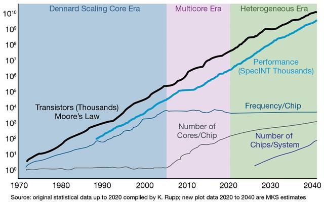
Figure 1. The chart shows historic trends in microprocessor transistor density, performance, and architecture from 1970 to the present, and projected through 2040. Courtesy of MKS.
Starting around 1970, manufacturers steadily increased processor performance by leveraging Dennard scaling, also called MOSFET scaling. According to this principle, as transistors shrink, their power density remains constant because their voltage and current scale down proportionally. As a result, processors could be made smaller and faster without excessive power consumption or overheating.
Dennard scaling served as a viable principle for manufacturers until around 2005. It ultimately broke because the leakage current does not scale down with size, which leads to heat dissipation issues. Simply increasing clock speed (frequency) was no longer a way to improve the performance of single-core processors or central processing units (CPUs).
Next, manufacturers turned to multicore architectures. Instead of making a single core faster, they integrated multiple cores on a single chip, allowing workloads to be distributed across them. This increased overall processing power while keeping both power consumption and heat dissipation within manageable limits.
The multicore approach was effective for about 15 years. But power consumption still increased as more cores were added. Again, thermal and power dissipation constraints became limiting factors, preventing further performance scaling using multicore CPUs alone.
Heterogeneous packaging is the next technological evolution that has been introduced to overcome this limitation. This concept integrates multiple specialized chips into a single package in a way that allows them to act like a single chip. Heterogeneous packaging enables continued performance gains for the overall package despite the slowdown of traditional transistor scaling.
This key innovation is often referred to as More than Moore, and it is helping to maintain the trajectory originally predicted by Moore’s law.
Heterogeneous computing: The benefits
The move to heterogeneous computing is especially crucial for AI applications because they benefit significantly from parallel processing. As a result, an AI package might integrate CPUs, graphics processing units (GPUs), and multiple high-speed memory chips to boost overall performance.
However, heterogeneous computing is only beneficial if all the integrated circuits in a package function essentially as a single chip.
Figure 2 shows a typical heterogeneous package configuration, such as one that might be used for AI. A logic chip(s), such as a CPU(s) or GPU(s), is at the top, along with a high-bandwidth memory module. The high-bandwidth module consists of multiple stacked dynamic random-access memory dies, connected vertically using copper-filled through-silicon vias to enable high-speed, low-power memory access. All of these components are electrically connected through a silicon interposer.
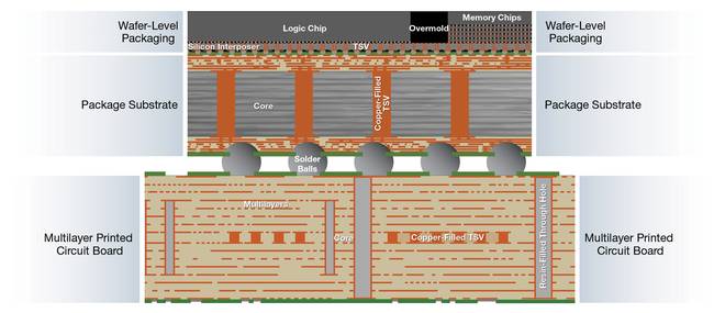
Figure 2. A simplified schematic of the cross section of advanced packages typical of AI applications. TSV: through-silicon via. Courtesy of MKS.
This entire assembly is mounted on a package substrate — a high-density interconnect structure that serves as the bridge between the chips and the multilayer printed circuit board (PCB). Unlike traditional PCBs, package substrates are specifically engineered for the fine-pitch, high-performance interconnects required in advanced semiconductor packaging. Several package substrates can be placed on a multilayer PCB and interconnected to behave as one chip.
By physically bringing these components closer together, heterogeneous packaging reduces latency, improves power efficiency, and enhances scalability. Additionally, the large number of interconnects used in advanced packaging is key to its performance.
Photonics keys heterogeneous packaging
A major challenge in manufacturing advanced packages is forming all of the necessary vias (holes) that connect each of the individual layers. This must be accomplished with increasingly challenging positional accuracy, hole shape quality, and at market-enabling speeds.
Photonics and laser drilling provide the best solution to many of the most demanding interconnect fabrication issues. Laser drilling is not new. For example, Electro Scientific Industries Inc., which MKS acquired in 2019, has supplied laser drilling systems to the electronics industry for more than 40 years. Still, steady increases in speed, accuracy, and hole quality have been necessary to keep pace with the demands for advanced packaging applications. The earliest via drilling systems simply moved the part relative to the laser beam using stepper motors. This allowed for speeds of ~100 holes/s. The next evolution was to add galvanometer scanners in combination with stage motion. This brought speeds up to ~1000 holes/s. But that value, too, was not fast enough for current advanced packaging production lines.
While photonics plays a critical role in achieving the precision and quality required for advanced semiconductor manufacturing, it does not operate in isolation.
To meet the needs of the highest throughput applications, MKS added an acousto-optic deflector into the system. The acousto-optic deflector element makes small, highly precise beam deflections at high speeds to improve both throughput and accuracy. The advanced packaging systems that use this technology can achieve drilling speeds of >10,000 holes/s.
Another important technology for advanced packaging production is precision motion. Typically, this involves high-precision positioning of components or test probes, often guided by machine vision, to accurately place and align them during assembly and testing.
Newport Corporation, which MKS acquired in 2016, is a leader in this area and continues to innovate in precision motion. Again, the present technology environment necessitates continuous improvements to the speed, accuracy, and stability of motion systems to support the most demanding advanced packaging production applications.
Accelerating the road map
Photonics will continue to drive innovation in semiconductor manufacturing — not only as a stand-alone technology but as an integral part of a broader, more interconnected ecosystem. By addressing markets for wafer fabrication equipment, package substrates, and PCB manufacturing, MKS aims to continue expanding its capabilities to ensure that as the industry evolves, the company is positioned to help shape its future.
Individual capabilities are key to meeting this goal; these include laser development and manufacturing as well as the supply of precision motion equipment.
However, this only addresses some reaches of the value chain. MKS acquired Atotech, a specialist in chemistry plating solutions, in 2022. The company supplies advanced plating equipment for the PCB industry and associated chemistry.
While photonics plays a critical role in achieving the precision and quality required for advanced semiconductor manufacturing, it does not operate in isolation. Broader technological capabilities such as via plating chemistry and equipment enable the development of solutions with greater efficiency, ultimately helping customers to achieve a faster time-to-market.