System Senses Individual Electrons
Kathleen G. TattersonMURRAY HILL, N.J. -- A system that can monitor and image individual electrical charges on and below the surface of semiconductor devices could be the next step in the never-ending quest for smaller, more powerful integrated circuits.
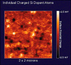
Scientists at Bell Laboratories have combined technologies from their single-electron transistor and the scanning probe microscope to develop the single-electron transistor scanning electrometer. According to the Bell Labs team, the technology will help bring forth the day when only a handful of electrons will control a device's performance. The instrument could aid in locating charged dopant atoms in semiconductor material. Typically, a single-electron microscope senses the combined electric field of up to 300 electrons at one time, explained Harald F. Hess, a researcher at Bell Labs.
"The location and the amount of dopants and how they release electrons is critical to device performance," he said. With the electrometer, scientists can image such charges with improved sensitivity.

The single-electron transistor scanning electrometer can produce images of single electrons and even small fractions of electrons. |
The probe is made of a sharpened glass fiber that looks like a sewing needle, onto which scientists have planted the device's circuitry. Its fine tip tapers to a small, almost flat area at the end measuring 100-nm wide. When near a semiconductor or other surface, the probe picks up small signals and measures the total charge to a small fraction of an electron. An "electric" image of the charge distribution emerges as the probe scans back and forth over the area.
Hess considers the device a research tool and said that the technology will not be ready for commercialization for another 10 years. "By pushing the frontiers of technology this far, we gain expertise and insight for closely related, more applied measurement problems," he said. The team is working to shrink the device, make it operate in a more realistic environment (it operates at only cryogenic temperatures of 2458 °F) and produce images with finer details.
LATEST NEWS
- Fraunhofer CAP Appoints Head, Scientific Director: People in the News: 1/15/25 Jan 15, 2025
- Bioluminescent Tags Track RNA Dynamics in Live Cells in Real Time Jan 15, 2025
- Sensing and Inspection Specialist EVK Joins Headwall Group Jan 14, 2025
- PHOTON IP Raises $4.9M Seed Round Jan 14, 2025
- Graphene Prevents Damage to Flexible Thin Films for Wearable Electronics Jan 14, 2025
- Thorlabs Acquires VCSEL Developer, Longtime Partner Praevium Research Jan 13, 2025
- Photoactivated Gel Achieves Bone Regeneration and Adhesion at Same Time Jan 13, 2025
- Electrically-Pumped GaAs-Based Nano-Ridge Lasers Fabricated at Wafer Scale Jan 13, 2025
