
Nano whispering gallery reduces semiconductor emission lifetime
Ashley N. Paddock,
ashley.paddock@photonics.comApplying the concept of whispering galleries to nanoscale devices drastically reduces emission lifetimes, a key property of light-emitting semiconductors, and shows great potential for the development of new ultrafast photonic devices.
Whispering galleries are circular chambers built into cathedrals by Renaissance architects; they are designed to reflect and direct sound waves so that a whisper can be heard from across the room.
When semiconductors are excited, it takes a few nanoseconds for them to return to the ground state, which is accompanied by an emission of light. This is known as an emission lifetime. For modulators, which switch back and forth, the emission lifetime sets a limit to the switching rate. The novel method reduces the emission lifetime to less than a picosecond – more than 1000 times faster than anything currently available.
The unique construction of the nano-wires developed by scientists at the University of Pennsylvania is the key to the reduced emission lifetimes. They have a cadmium sulfide core surrounded by a buffer layer of silicon dioxide and an outer layer of silver. The silver layer supports surface plasmons – unique waves that consist of a combination of light and oscillating metal electrons. The surface plasmons are highly confined to the surface, where the silver layers and silicon dioxide meet.
Previous research placed the nanowires on a metal surface; the new method wraps the metal surface around the wire to form a nanoscale plasmonic cavity, which achieves the whispering gallery effect.
“There has been some interesting work on nanowires assembled on metal substrates, so we wanted to see what would happen if we made an integrated structure where the metal was coated on the nano-wire,” said Ritesh Agarwal, associate professor at UPenn.
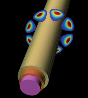
A rendering of the triple-layered nanowire and whispering gallery electromagnetic fields.
Courtesy of Ritesh Agarwal, University of Pennsylvania.
For certain nanowire sizes, resonance pockets were formed in the silver coating layer, resulting in highly confined electromagnetic fields within the nanostructure. The emission lifetime can then be engineered by precisely controlling the electromagnetic fields inside the light-emitting cadmium sulfide core.
Quality and confinement
To achieve an emission lifetime in the femtosecond range, the researchers optimally balanced the high-confinement electromagnetic field with an appropriate quality factor, a measurement of how good a cavity is at storing energy; quality factors and confinement are inversely related. By opting for a moderate quality factor, the researchers increased the confinement of the electric field inside the nanowire by using resonant surface plasmons and achieving a record-breaking emission lifetime.
“We did anticipate significant changes in the optical properties of the nanowire-plasmonic system due to the strong confinement, but still, the thousandfold decrease in the excited-state lifetime of semiconductors was surprising to us,” Agarwal said.
The results were published online July 17 in
Nature Materials (
doi: 10.1038/nmat3067). The scientists hope that this improvement can be used in a variety of applications, including optical computing devices operating in the terahertz range.
“In addition to making LEDs, modulators, switches and photovoltaic devices, we would like to study the ultimate limit of how much light-matter interaction can be manipulated in these ultrasmall structures,” he said. “Active plasmonics is an emerging field, and these types of novel structures will be critical to drive this field because the diameter of nanowires (unlike nanocrystals) is in the right range to obtain confined optical cavity modes.”
LATEST NEWS
