Future Looks Bright for Sol-Gel Techniques
Kevin RobinsonJENA, Germany -- Seven European partners have completed a three-year project to develop sol-gel processing techniques for waveguides, lens arrays, waveguide amplifiers, electro-optical modulators, switches and other elements. The goal was to develop these techniques to introduce lower-cost manufacturing methods for optical components.
According to Steffen Goerlich of Jenoptik L.O.S. GmbH in Jena, traditional waveguide technologies, such as ion exchange in glasses and titanium diffusion in lithium niobate, are relatively costly, especially when the production quantities are small. The sol-gel process, he said, has the potential to produce less-expensive elements containing fiber alignment structures.
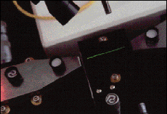
Researchers created an optical amplifier channel, visible in the green upconversion light, from a sol-gel process similar to semiconductor manufacturing processes. Courtesy of Robert Bosch GmbH. |
Cheaper components
In the sol-gel process, manufacturers use bulk liquids to produce organic or organic-inorganic composite materials with stable, nano-size particles. The process builds up, bit by bit, a stable, three-dimensional body. The benefits of the process are that the products' quality can be controlled by ensuring the purity of the basic materials and that the optical properties can be tailored easily by doping the basic materials or adding colloidal particles.
The group embossed the structure of a Fresnel lens array for a fiber measuring head into a network of organic and inorganic components that contained SiO2 nanoparticles. According to Goerlich, optical tests measured the diffraction efficiency at 60 to 65 percent. In addition to this and other components, the group created optically addressed Mach-Zehnder and Jamin interferometers and a fast optical switch using the optical dependence of refractive index in gold quantum dot doped sol-gel films. Goerlich listed many applications that can benefit from sol-gel processes including telecommunication waveguides, micro-optics and waveguide amplifiers.
Goerlich said the group will continue basic material research, but also will begin other experiments such as environmental tests of microstructures and integrating additional elements into the waveguide amplification chips. "Our main goal," he explained, "is to inform interested people of the technical possibilities for manufacturing high-quality optical components using the sol-gel technique." The project was funded by the Commission of the European Community.
LATEST NEWS
- Fraunhofer CAP Appoints Head, Scientific Director: People in the News: 1/15/25 Jan 15, 2025
- Bioluminescent Tags Track RNA Dynamics in Live Cells in Real Time Jan 15, 2025
- Sensing and Inspection Specialist EVK Joins Headwall Group Jan 14, 2025
- PHOTON IP Raises $4.9M Seed Round Jan 14, 2025
- Graphene Prevents Damage to Flexible Thin Films for Wearable Electronics Jan 14, 2025
- Thorlabs Acquires VCSEL Developer, Longtime Partner Praevium Research Jan 13, 2025
- Electrically-Pumped GaAs-Based Nano-Ridge Lasers Fabricated at Wafer Scale Jan 13, 2025
- Photoactivated Gel Achieves Bone Regeneration and Adhesion at Same Time Jan 13, 2025