Luc Augustin,1-2 Meint Smit,1 Norbert Grote,3 Mike Wale1-4 and Richard Visser,2 1Eindhoven University of Technology; 2Smart Photonics BV; 3Fraunhofer HHI; 4Oclaro
A generic foundry approach could result in a dramatic cost reduction for production of PICs for a variety of applications.
A revolution is coming in photonic integration technology, facilitated by the introduction of generic foundry processes: highly standardized photonic integration processes that enable realization of a broad range of application-specific photonic integrated circuits (ASPICs) from a small set of basic building blocks. This will lead to a dramatic reduction of the development costs of photonic integrated circuits (PICs), which will bring them within reach for small and medium enterprises (SMEs), universities and research institutes. The revolution will be similar to the one that took place for ASICs (application-specific integrated circuits) in microelectronics more than three decades ago.
Indium phosphide (InP) – the material of choice for lasers and amplifiers in the telecommunications wavelengths – and silicon photonics are the two major technologies for the development of complex high-performance PICs. InP photonics platforms offer full monolithic integration of active and passive devices in a generic integration process. Europe is clearly leading in the deployment of this technology, with three foundries offering InP-based photonic foundry service on a commercial basis. Generic foundry processes and the infrastructure to make them accessible at low cost for a broad range of companies (design tools, component libraries) are being developed, and first versions are now available for beta-type access by external customers. Development is ongoing to realize generic packaging technology and generic test facilities.
Generic foundry process
The first complex PICs were published around 1989,1 and despite similarities in the development of chip complexity with microelectronics, there is a remarkable difference in the R&D methodology followed. In photonics, most integration technologies are developed and optimized for a specific device or application. As a result, there are almost as many technologies as applications, most of them very similar, but sufficiently different to prevent easy transfer of a design from one fab to another. Because of this huge fragmentation, the market for many of these device-specific technologies is too small to justify their further development into a low-cost industrial volume manufacturing process. As a result, chip costs remain too high to find wide application.
A dramatic cost reduction can be achieved if the chip design is based on a generic (standardized) integration process.2 Generic processes allow for fast prototyping and low costs, as no process development is required. The performance and functionality of the processes that are developed can meet in many respects with the best device-specific processes that are currently exploited.
Furthermore, a significant cost reduction in the development phase is achieved by making use of multiproject wafer (MPW) runs. In these MPW runs, a number of users share the same wafer and hence share the fabrication costs. This way of working is both financially and technically attractive, as no large investments, no expensive and lengthy process development, and no in-depth knowledge of the technology are required for the user.
In this approach, entry costs are mainly restricted to design costs, which can be on the order of €100,000. Such expenses are affordable for many SMEs, and the introduction of the generic model will lead to a rapid expansion of the application of InP-based ASPICs. For production purposes, cost levels of €10/mm2 can be reached already at volumes of 1000 chips.
In 2007, this photonic foundry approach was proposed by the Network of Excellence ePIXnet, and three technology platforms were established: The JePPIX platform for InP photonics, the ePIXfab platform for silicon photonics and, later, the TriPleX platform for low-loss dielectric waveguide technology for application in the visible-to-IR wavelengths.
The European JePPIX consortium is working with three InP PIC platforms to extend their capabilities and offer them to a wider user base. The platforms are currently in an advanced development stage, and commercial offerings are planned; the first commercial InP MPW started in June.
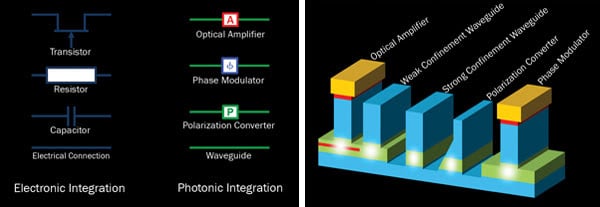
Figure 1. A generic foundry process could open up photonic integrated circuits (PICs) to much wider availability. The generic photonic integration philosophy (a), and a schematic drawing of building blocks in an integration platform (b). Courtesy of COBRA Research Institute, Eindhoven.
As part of JePPIX, the COBRA Research Institute at TU Eindhoven started pioneering small-scale access to MPW runs for research purposes. Since 2009, the European EuroPIC and PARADIGM projects have been working on transfer of the foundry model from a university environment to an industrial environment – the platform technologies of Oclaro and Fraunhofer HHI. In 2012, SMART Photonics joined the JePPIX platform and has started offering commercial access to the COBRA generic integration process.
Technology
This generic integration model is very similar to the approach in microelectronics, where a huge market is served by a relatively small set of integration technologies (most of them CMOS technologies). For these technologies, a broad range of functionalities can be realized from a small set of basic building blocks such as transistors, resistors, capacitors and
interconnection tracks. By connecting these building blocks in different numbers and topologies, we can realize a huge variety of circuits and systems, with complexities ranging from a few hundred to more than 1 billion transistors. In photonics, we can do something similar. With the basic building blocks as given in Figure 1 (waveguides, semiconductor amplifiers, phase modulators and polarization converters), we can make a wide variety of components.
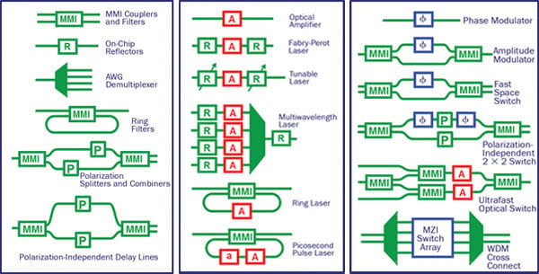
Figure 2. Examples of composite building blocks using the generic integration technology. MMI = multimode interference; MZI = Mach-Zehnder Interferometer; AWG = arrayed-waveguide grating; WDM = wavelength division multiplexing. Courtesy of COBRA Research Institute, Eindhoven.
This is demonstrated in Figure 2. With waveguides alone, we can make not only interconnections, but also passive components such as couplers, filters and demultiplexers. If we also integrate optical amplifiers, phase modulators and polarization converters for manipulating the amplitude, the phase and the polarization of the light, we can control all properties of the light.
Figure 3 summarizes the differences between the technologies currently available: silicon photonics, InP-based monolithic integration and TriPleX for low-loss dielectric waveguide technology. InP is the platform of choice for the integration of lasers and optical amplifiers – it is very complementary to TriPleX – and a hybrid platform combining the two would offer outstanding capabilities by combining superior active functionality (lasers, amplifiers, modulators, detectors) with superior passive functionality (very low-loss waveguides, high-Q filter, dense demultiplexers, etc.).
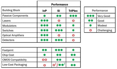
Figure 3. Comparison of three different technology platforms. Courtesy of COBRA Research Institute, Eindhoven. 1 = end-fire coupling (low reflection); 2 = vertical coupling (medium reflection).
Software
For the generic process to be successful, design software is required in addition to the process technology. This is developed by software partners to allow an easier and faster design method based on the building blocks. The most important aspect of this is the development of process design kits for every foundry process. The design kit contains two important parts: a component library in which all properties of the building blocks are described, and general design rules for fabrication in the platform. Ideally, a component library module contains a part for simulating the component performance and a part for generating the mask layout.
Multiproject wafers
The standardization of the process has another big advantage. Because the process is the same for all ASPICs, their processing can be combined on the same single wafer. These MPWs offer a large cost advantage for the users, as they all share the cost of a single run. This brings the technology within reach not only for large companies but also for SMEs. Figure 4 shows a fully processed MPW in the COBRA process, and the different ASPICs from different users are visible in this wafer.
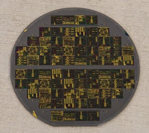
Figure 4. This multiproject wafer contains 12 user designs. Courtesy of COBRA Research Institute, Eindhoven.
The MPW runs are planned for all foundries, and users can subscribe to their platform of choice. Potential designers get access to the foundry’s process design kit and can create the designs for user applications. Design houses will take care of the designs, and the designs are collected by a broker and compiled to fit in one run in a foundry.
Applications
Many companies could profit from access to generic fabrication of PICs, which would open up a whole new range of applications. Figure 5 shows that a broad range of applications is covered: telecom and other lasers, plus medical applications (OCT, pulse shapers for bioimaging), sensors (readout units for fiber sensors), and FTTH applications are demonstrated.
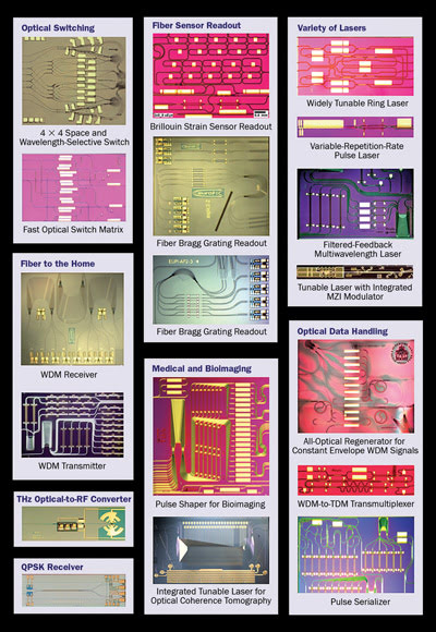
Figure 5. An example of ASPICs fabricated with generic integration technology. Courtesy of Fraunhofer HHI, Oclaro, COBRA Research Institute, and platform users in EuroPIC and PARADIGM. QPSK = quadrature phase-shift keying; TDM = time division multiplexing.
Meet the authors
Luc Augustin is JePPIX coordinator at COBRA Research Institute of Eindhoven University of Technology in the Netherlands and process architect at SMART Photonics BV, also in Eindhoven; email: [email protected]. Meint Smit is a professor at the COBRA Research Institute; email: [email protected]. Norbert Grote is deputy head of the photonics department at Fraunhofer HHI in Berlin; email: [email protected]. Mike Wale is a professor at the COBRA Research Institute and director of active products research at Oclaro in Caswell, England; email: [email protected]. Richard Visser is CEO at SMART Photonics BV; email: [email protected]. The authors would like to gratefully acknowledge support from EU projects EuroPIC (NMP 228839) and PARADIGM (ICT 257210).
References
1. U. Koren et al (May 1989). Wavelength division multiplexing light source with integrated quantum well tunable lasers and optical amplifiers. Appl Phys Lett, Vol. 54, pp. 2056-2058.
2. M. Smit et al (March 2011). Generic foundry model for InP-based photonics. IET Optoelectron, Vol. 5, pp. 187-194.