Photonic integrated circuits reject the ideal of the all-optical network in favor of embracing low-cost optical-electrical-optical conversion.
Jeff Ferry, Jacco L. Pleumeekers, Atul Mathur, Andrew G. Dentai and Peter W. Evans, Infinera Corp.
Over the past two decades, telecommunications operators worldwide have deployed fiber optic networks with progressively larger bandwidth capacities. Two of the most significant innovations in these networks in the 1990s were dense wavelength division multiplexing (DWDM) and optical amplifiers, which enabled multiple wavelengths or channels of light to be amplified without demultiplexing. By the mid-1990s, DWDM networks were widespread, especially in long-haul networks in North America, Europe and Asia.
Optical impairments set in after a certain distance, requiring that an optical signal be demultiplexed, converted to the electronic domain, “cleaned up” and then converted back to the optical domain before beginning the next leg of its journey through the fiber. This process, known as optical-electrical-optical regeneration, remains a major cost factor for telecom service providers building optical networks.
A representative architecture is illustrated in Figure 1. In this example, a provider is sending traffic between New York and Washington. The limitations of the optical system require the deployment of regenerators at three locations between the cities. In the illustration, there are four wavelengths (shown as different colors) on this route, but 40 or 80 are not uncommon in real-world networks.

Figure 1. A typical optical link in a telecom network requires optical-electrical-optical (O-E-O) regeneration at regular intervals, either to serve customers at those add/drop points or because of degradation in the optical signal.
All-optical ideal
With such large channel counts, the cost of each optical-electrical-optical regenerator site could easily top $1 million or $2 million. The elimination of these regenerators thus became a critical objective for the optical networking industry.
For most in the industry, eliminating optical-electrical-optical regeneration meant developing ways to maintain the signal in the optical domain for longer and longer distances. The “all-optical network” became something of a mantra, particularly in the Internet’s boom years of 1998 to 2001. Start-ups and large companies introduced technologies to move the industry closer to the all-optical goal. Established equipment makers improved the performance of their systems to stretch optical reach from 500 to 600 km in the mid-1990s to 1000 to 1500 km today, while “ultralong haul” systems have optical reaches of 2000 to 3000 km.
However, these new products or architectures brought with them several disadvantages. For one, longer optical reaches limited the ability to offer services to customers in intermediate cities. If a service provider built that New York-to-Washington route without optical-electrical-optical regeneration, what would it do a year later if customer opportunities arose in Baltimore, Philadelphia, or Newark or New Brunswick, N.J.?
Other problems with the all-optical architecture included the inability to reliably monitor performance of the network except at the optical-electrical-optical points or terminals. When the optical signal is converted to electronic bits, its performance can be monitored; in the optical domain, it is impossible — at least with current technology — to evaluate the quality of the digital data.
Finally, the engineering requirements of very long optical reaches introduce added costs and complexity to managing the network. Complex engineering often is required to monitor and adjust power levels, compensate dispersion and address other impairments at many points along the route.
Rethinking regeneration
Infinera Corp. of Sunnyvale, Calif., took a different approach to the problem. The company’s engineers believed that reducing the cost of optical-electrical-optical regeneration would be a better solution than eliminating the technology.
If regeneration could be retained at frequent nodes in the network at dramatically reduced cost, it would bring with it all the advantages of electronic access to the digital data. Those advantages include the ability to switch and groom the signal, monitor performance, add and drop services at many points on the network and provide restoration, and they enable service providers to offer valuable commitments — such as network uptime commitments — to their customers. Many of these features not only would improve network performance, but also would create immediate revenue opportunities for carriers.
In 2004, Infinera introduced its first large-scale photonic integrated circuits, or PICs, semiconductors with approximately 50 optical components on each chip. It produces two versions: a transmit and a receive PIC (Figure 2).
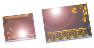
Figure 2. Left: The receive photonic integrated circuit (PIC) receives 10 10-Gb/s optical signals on a single fiber input, demultiplexes them and converts them into a 100-Gb/s electrical signal. Right: The transmit PIC receives one 100-Gb/s electrical signal, converts it to 10 10-Gb/s optical signals, multiplexes them at standard C-band wavelengths and transmits them onto a single fiber. Each PIC contains approximately 50 optical components.
The transmit PIC comprises 10 lasers, 10 modulators, variable optical attenuators and other components, all on a chip that is smaller than a human fingernail. The receive PIC includes 10 photoreceivers and many other components on a slightly smaller chip. The pair is mounted on a line card, the digital line module, each with a capacity to manage 100 Gb/s.
Thanks to the integration of so many components onto the PICs, a digital line module significantly lowers the cost barrier to digital regeneration and manipulation of data while delivering 10 times the capacity of other optical networking systems, which typically are based on 10-Gb/s line cards.
The PIC required advances in design and production. Previously, two or three optical components had been designed on the same substrate, but there had been no previous efforts at the monolithic integration of optical components on this scale. Moreover, the technology, tool set and experience in the III-V semiconductor industry are years behind that in the silicon industry, so integrating multiple components onto a single InP substrate involved the development of techniques for multiple epitaxial regrowth, active-active and active-passive transitions, and electrical-optical isolation.
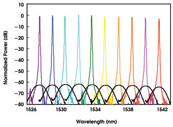
Figure 3. PIC lasers emit radiation locked to the standard ITU grid and at similar power levels. An on-chip variable optical attenuator equalizes the power level in all channels. The passbands for the multiplexer on this chip are shown in black.
The transmit PIC operates at a channel spacing of 200 GHz (Figure 3). Its lasers emit at similar power levels and are closely locked to the ITU grid, enabling them to operate to the same specifications as standard carrier-class telecom equipment. The use of multiple PICs at different wavelength grids enables the system to achieve channel spacings of 50 GHz.
The link characteristics of the PICs have been tested over distances typical of conventional long-haul telecom networks. The channels maintain open eye diagrams, indicating acceptable signal-to-noise ratios, and maximum peak-to-peak jitter of less than 12 ps (Figure 4).
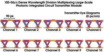
Figure 4. Eye diagrams show good signal fidelity in operation over a long-haul network span.
The company chose not to market the PICs as stand-alone products but rather to build a complete optical transport system based on them. This enabled the designers and systems teams to optimize the design for the marketplace. For example, it was judged that a two- or three-channel PIC would not offer sufficient benefits to justify the investment in the technology. Therefore, a 10-channel PIC was targeted. Perhaps the most significant decision was not to compartmentalize product design and manufacturing, but to develop product specifications and manufacturing technology in tandem.
The optical network system built around the PIC can be superior to conventional long-haul optical systems in terms of initial cost, space and power consumption. Over time, standard semiconductor economics will come into play. Yield will rise, and costs will decline, bringing further advantages to the PIC-based system.
Evidence of the technology’s benefits include the fact that the optical system, which originally was introduced as a long-haul solution, has found customers in the metro market, which typically involves point-to-point networks or rings in cities, with nodes spaced from two to 50 miles apart.
‘Optical Moore’s law’
The photonic semiconductor industry has been slower to develop than the silicon semiconductor industry, but it is gathering speed, as photonic integration has become economical for many networks and as production processes have advanced to enable the cost-effective production of increasingly complex PICs.
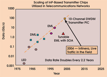
Figure 5. The data rate has doubled every 2.2 years since the introduction of LEDs in the 1970s. The 100-Gb/s PICs are widely deployed today, and a 400-Gb/s device was demonstrated in 2005. DML: Directly modulated laser. EML: Electroabsorption-modulated laser. SOA: Semiconductor optical amplifier.
Figure 5 plots the progress in the data rate for photonic devices from the first LEDs in the mid-1970s. Notable points include the introduction of the 10-Gb/s line-rate into telecom networks in 1996, and Infinera’s introduction of the 100-Gb/s PIC into live telecom networks in late 2004. Last year, the company reported the successful testing of a 400-Gb/s PIC based on 10 channels transmitting data at a 40-Gb/s rate. The trend line plotted on the graph shows that the data rate has doubled every 2.2 years. Dubbed the “optical Moore’s law,” this is one-third slower than Moore’s law but impressive nonetheless.
Meet the authors
Jeff Ferry is director of communications, Jacco L. Pleumeekers is a process integration engineer, Atul Mathur is a member of the technical staff, Andrew G. Dentai is an epi engineer, and Peter W. Evans is an integration engineer, all at Infinera Corp. in Sunnyvale, Calif.; e-mail: [email protected].