Full company details
Edmund Optics Inc.
 101 E Gloucester Pike
Barrington, NJ 08007
United States
Phone: +1 856-547-3488
Fax: +1 856-573-6295
Toll-free: +1 800-363-1992
Techspec Fused Silica Wafers
Photonics.com
Jul 2014BARRINGTON, N.J., July 25, 2014 —
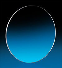
With less than 10-Å surface roughness, Techspec Fused Silica Wafers from Edmund Optics can be used as test substrates for measuring optical coating quality.
The thin, circular pieces of UV-fused silica provide 40-20 surface quality with RoHS compliancy. All wafers have thicknesses of 1 mm and a transmission range of 0.2 to 2.2 µm.
Techspec wafers are ultrasonically cleaned and can also be used in semiconductor microlithography, micro-electrical-optical applications or set-up processes as dummy components.
More products