
University Spinoff to Advance Optical Integration
A recent spinoff from the Technical University of Valencia is looking to further optical integration by increasing the complexity of chip designs and improving fabrication processes.
Optical integration has followed the steps of microelectronic integration for almost a decade now: Bulk optical components such as lasers or photodetectors have been miniaturized into a chip, with corresponding reductions in size, weight and, especially, cost.
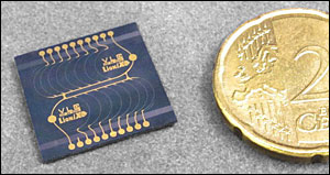
VLC Photonics is looking to further optical integration. Pictured is one of the company's photonic integrated circuits for optical telecommunications, fabricated in silicon nitride. (Images: VLS Photonics)
Fabless manufacturing mimics the electronic integration model, where specialized foundries provide exclusive chip fabrication services to design houses, including the new spinoff, VLC Photonics. This allows for very efficient, standardized and reliable manufacturing processes, and ensures large cost reductions due to economies of scale. On the other side, the optical chip design houses open the doors of integration to large and small companies and institutions that might not have, or need, the required optical knowledge and circuit design expertise.
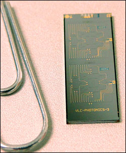
Advanced optical systems can be embedded into a single chip by using silicon or more exotic substrate materials, including indium phosphide. Here, a photonic integrated circuit for optical telecommunications fabricated in indium phosphide.
"Traditionally, optical component vendors have internally developed fabs and processes to optimize their manufacturing of specific devices, like lasers or modulators. The emerging fabless paradigm calls for open foundries that can provide generic building blocks to build complex chips by external users," said Pascual Muñoz, CEO of VLC Photonics. "We can now embed advanced optical systems including tens to hundreds of devices into a single chip by using silicon-based and more exotic substrate materials like indium phosphide."
For these materials, new foundries have been established in recent years through publicly funded research institutions; privately held companies have been the engine behind others. Europe currently leads this trend, with the US and Singapore closely behind. Besides dedicated fabrication runs, some of these institutions offer multiple shared-access integration platforms that allow for low-cost fabrication by sharing wafer space among different designers; examples include the EC-funded ePIXfab for silicon, and JePPIX and TripleX for other types of substrates.
"Design houses can then choose to either specialize on a single platform or, like VLC Photonics, be skilled in multiple technologies and design for the most suited material depending on the customer's end application," Muñoz said.
This new model of operation evolved from the traditional research-based one, where each university or R&D department had its own custom fabrication process and could not deliver industrial-grade production if required. Such successful transfer from academia to the commercial world enables photonic integrated circuit applications that are as numerous and varied as their electronic counterparts: from telecommunications to sensors, biomedicine to information processing and more.
For more information, visit: www.vlcphotonics.com
Published: September 2012