As they get faster and offer higher resolution and sensitivity, CMOS sensors continue to impress the manufacturing industry.
The main goal of any industrial inspection system is to increase manufacturing efficiency as measured by throughput, yield and number of product returns. Inspection systems are therefore pressed for continual improvements in speed, resolution and power consumption as well as capital cost.
CMOS sensors offer increasingly high frame rates and are very attractive for high-speed applications.
Greater speed allows manufacturers to see physical characteristics when an object is moving very fast or is highly magnified. Better resolution means higher spatial resolution and greater detail in the images, and increased light sensitivity means that this can be done with minimal investment in supplemental lighting.
“Image sensors are the eyes of optical inspection systems,” said Eric Fox, technical director of CMOS integrated circuits at Teledyne Dalsa in Waterloo, Ontario, Canada. “Without advances in the performance of image sensors, it is not possible to exploit parallel advances in illumination, data transmission, image-processing hardware and image-processing software.”
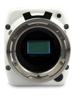
Higher speed, resolution and sensitivity are top goals at Vision Research, and the company says CMOS will help it achieve those goals. This picture of the Miro M-series camera without the lens reveals the CMOS sensor beneath.
Of course, this applies to all image sensors, but in particular to those based on CMOS technology, as these are fast becoming the technology of choice for inspection.
“There are three characteristics of the sensor that we continue to advance: speed, resolution, sensitivity,” said Rick Robinson, director of marketing at Vision Research, a high-speed digital camera maker in Wayne, N.J. “And these are engineering trade-offs – it is nearly impossible to advance all three simultaneously. And all three can benefit inspection applications.”
But speed, resolution and sensitivity aren’t everything: Other attributes also are helping to make CMOS sensors an increasing asset on the production line.
Global electronic shutters provide crisp, blur-free images of fast-moving objects without the need for a mechanical shutter or pulsed illumination. Reductions in read noise and in the effects of shot noise also contribute to image quality – and in some cases can enhance the quality of the products. This can be seen, for example, in the solar panel market, where efficiencies continue to increase and costs continue to decrease over time.
Imaging modules incorporating Sony’s Exmor RS, the world’s first stacked CMOS image sensor. Its sensor section and circuit section are laid one on the other on a silicon wafer supporting substrate.
“Teledyne Dalsa has been in the business of developing new and better image sensors to advance inspection capabilities for over 30 years. Throughout, the drivers have remained the same: Run faster, with more resolution, with higher sensitivity, at lower cost,” Fox said. “Over the past 10 to 15 years, power consumption has been added to that list of drivers as system sizes have scaled down in size.”
Most recently, the company has released the Genie TS and Falcon2 CMOS sensor cameras for area-scan applications, the Piranha4 8k for line scanning and the Piranha HS NIR for time delay and integration (TDI) applications.
CMOS technology will be as successful in line-scan applications as it has been in area-scan applications, said Jana Bartels, product manager for digital camera manufacturer Basler AG in Hamburg, Germany. The company is putting a lot of effort into developing cameras with its partners Cmosis, Aptina Imaging Corp., Awaiba CH SA and e2v.
The Genie camera from Teledyne Dalsa features a 1.4-megapixel, 100-fps CMOS sensor packaged on FR4 material to help minimize cost.
For example, the latest digital line-scan sensors with 24-k (24,576 pixels) resolution from Awaiba of Yverdon, Switzerland, offer inspection of fine defects at high throughput speed. This is particularly useful in the manufacturing of solar cell substrates, especially thin-film solar cells, and in production inspection of LEDs and LCDs.
“A completely different product innovation is our world-smallest global shutter sensor, NanEye_GS, which provides in a form factor of only 3.4 x 3.4 mm a global shutter sensor that can deliver 100 full images per second at 640 x 640-pixel resolution,” said Awaiba CEO Martin Wäny. “The sensor is ideal for compact vision systems such as data matrix code readers or intelligent light barriers.”
The rise and rise of CMOS
State-of-the-art CMOS image sensor(CIS) technology is reaching a point where its overall performance is comparable to that normally expected from CCD-based image sensors.
And some believe that CIS technology also is nipping at the heels of broadband and image intensifier devices such as those based on microchannel plates, photomultiplier tubes or similar technologies.
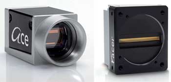
CMOS technology will be as useful for line-scan applications as it
has been for area-scan applications, according to the German company
Basler, which is developing new cameras. Here, the Basler Ace area-scan
cameras (left) are equipped with both CCD and CMOS sensor technology;
the company’s Racer line-scan cameras (right) use highly sensitive CMOS
sensor technology.
“Many of the cameras launched in the past year or two have been CMOS, and if you examine what is cooking in the R&D labs of most companies, you’ll find it is almost entirely CMOS,” Teledyne Dalsa’s Fox said. “Thus, for machine vision, I think the transition has happened, with the exception of TDI. We still sell a lot of TDI products because the architecture that CCDs allow is so ideally suited to the application.”
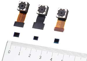
The NanEye CMOS image sensor has optics integrated into the package. Measuring just 1 x 1 x 1.4 mm, this module comprises a full digital camera functionality and works without any additional components at up to 3 m on a wire.
Although the image quality of CMOS image sensors has improved tremendously over the past 10 years, some off-chip digital processing is still necessary to get the best from the resulting image.
More and more of this will be integrated on chip so that CMOS image sensors will become easier for the customer to use.
This added functionality is one of the most important requirements for future CMOS sensors, according to officials at Sony Corp., where the sensors and modules are developed in a vertically integrated fashion, which it says provides customers with added value that is unique to Sony.
Developing superresolution zoom and a low-power autofocus actuator will enable advanced functionality and lower power consumption, the company said.
Sony has just released the Exmor RS. The conventional back-illuminated CMOS image sensor has the sensor and circuit sections on the same plane, with one section laid on the other on the supporting substrate of a silicon wafer.
Putting a circuit inside the supporting substrate uses that substrate more effectively, making the 1/4-inch system-on-chip image sensor about 40 percent smaller, the company said. Previously, sensor and logic – two incompatible processes – had to be built on the same plane; now that they can be separated, the conditions for each can be optimized, which Sony says enables better performance and image quality.
Future challenges
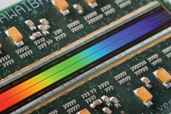
Along with the usual suspects of speed, resolution, sensitivity, image quality and power, we can expect to see advances in color imaging and in extending spectral responsivity to wavelengths outside the visible spectrum; today’s inspection applications increasingly make use of spectral information to detect defects.
Huge efforts also are being made to further decrease noise floors of the CIS, which increases its dynamic range and takes us a step closer to single-photon detection abilities.
“Nevertheless, if all the advantages of the mature CMOS technology are to be preserved, this can only be done through the integration of other detector materials into the CIS fabrication processes,” said Dr. Daniel Durini, group manager of Optoelectronic Devices at Fraunhofer Institute for Microelectronic Circuits and Systems in Duisburg, Germany. “This approach takes us into the world of 3-D hybrid sensors, where several layers of detector materials and readout circuits are integrated together, offering a complete new world of possibilities not existent so far.”
Near-single-photon counting with picosecond time resolution has been one of the main breakthroughs of the past couple of years, presented in the form of SiPM (silicon photomultipliers) or SPADs (single-photon avalanche diodes).
These technologies are very promising but still have many drawbacks, Durini said. The drawbacks include pixel sizes, dark count rates, dead times and fill factors in the case of SPADs, and the absence of spatial resolution, in the case of SiPMs. They all must be solved before commercialization is possible.
Three-dimensional imaging or high-performance ranging based on the time-of-flight principle also has made huge advances.
There are several competitors on the market right now, all waiting for the big breakthrough that could be coming soon, Durini said. “If sufficiently mature and advanced, this technology might open an enormous new world of uses, especially where machine vision and industrial applications are concerned.”
The merits of CMOS sensors, at a glance:
• Good full-well capacity
• Small sensor sizes (which means smaller cameras)
• High speed
• High image quality (comparable to CCD technology)
• No tap balancing
• Global shutter when capturing moving objects (prior to CMOS, this was possible only with more expensive
CCD sensors)
• Low noise resulting from new sensor developments
• New special features such as windowing and high-dynamic-range improvements
• Low system complexity
• High sensitivity in the NIR spectrum
• Less blooming than in CCD technology
• Less smear than in CCD technology (important when capturing moving objects)
• Extended functionality in one chip
• Low power consumption