The vast majority of optics used in precision scientific, industrial, biomedical, and military applications incorporate thin-film coatings on their surfaces. Therefore, it’s useful for almost anyone involved in the specification and purchase of optical components to have some familiarity with the typical performance characteristics, trade-offs and limitations of various coating types, as well as some knowledge of the capabilities of common thin-film production technologies. This article provides an objective overview of both these topics.
Trey Turner and Roger Kirschner, Research Electro-Optics Inc. (REO)
What are thin-film coatings? The purpose of any optical thin-film coating is to modify the transmittance and reflectance properties of the substrate material to which they are applied. Most coatings can be broadly classified into one of the following categories:
Antireflection (AR): These are used to suppress unwanted reflections that normally occur at the interface between two different materials, such as air and glass.
High reflection (HR): Mirror coatings are used to increase the reflectivity of a surface.
Partial reflection: Beamsplitters transmit a specified percentage of input light and reflect the rest. They are often used at nonzero angles of incidence.
Polarization: Polarizers separate incident light into orthogonally polarized components, typically transmitting one and reflecting the other.
Filter: These may perform any of the preceding functions, but on a wavelength-selective basis; for example, transmitting one wavelength and highly reflecting a second.
Optical coatings are constructed of either thin layers of dielectrics or a relatively thick layer of a metal, as well as combinations of both classes of materials. Metal coatings rely on the bulk reflectance and absorption characteristics of the coating material for their operation. In contrast, dielectric thin-film coatings operate by utilizing optical interference. A simplified schematic of how this works is shown in Figure 1, which depicts a light ray incident upon a material having a single-layer thin film on its surface. Part of the ray energy is reflected at the air-coating interface, and part of it is transmitted and refracted. At the coating-substrate interface, some energy is again reflected and transmitted. The two reflected rays overlap, and, since they are lightwaves, the amplitude of the reflected light is the complex sum of the amplitudes of the two overlapping rays.
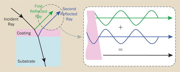
Figure 1. Schematic illustration of single-layer antireflection coating operation.
It is possible to arrange things so that the two reflected rays cancel each other out, meaning there is no reflection at all. This is an antireflection coating. This occurs when both the reflected rays have equal amplitude but are exactly one-half wave (180°) out of phase, resulting in destructive interference.
For the two rays to be out of phase, the second reflected ray must traverse an optical path length that is exactly half the wavelength of the light before they recombine. If the input ray is at normal (0°) incidence, the optical thickness of the coating must be one-quarter the wavelength to meet this condition. For the amplitudes of the two reflected rays to be identical, the index of refraction of the coating must be exactly the square root of the index of the substrate material.
However, these conditions can only be exactly satisfied at one wavelength and one angle of incidence. Furthermore, for many substrates, there may not be any suitable coating material that has exactly the necessary refractive index. So, while single-layer antireflection coatings are widely used, thin films for more demanding applications often consist of multiple layers. More complex, multilayer designs can deliver higher performance and enable operation over a wider range of wavelengths and incident angles, as well as permit the use of the most practical and readily available coating materials.
Practical coating trade-offs
Utilizing this basic principle of interference, multilayer dielectric coatings can be designed to suppress or enhance reflection at one or more wavelengths, or to preferentially reflect or transmit one polarization. Real-world coatings that accomplish these tasks can sometimes contain tens, or even hundreds, of layers, and are fabricated from numerous available materials.
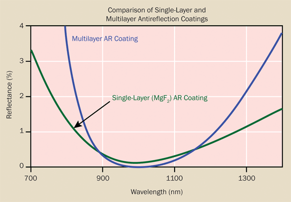
Figure 2. Adding layers to an antireflection coating lowers the reflectance but reduces the coating bandwidth.
However, the range of materials available to the coating designer is not infinite, meaning that practical coatings must be constructed using a limited set of refractive indices. Furthermore, these materials cannot be deposited with absolutely perfect control of their thickness and refractive index. It is therefore important for the coating buyer to understand what level of performance specifications can be achieved in practice, and what specifications tend to drive cost, or result in other undesirable outcomes, such as decreased mechanical durability or reduced laser damage resistance. The most common considerations for each of the coating types listed previously are reviewed here.
Antireflection coatings
Performance in an AR coating is typically specified by either the maximum allowable reflectance at a single wavelength or by the average allowable reflectance over a specified wavelength range. For AR coatings intended for a single wavelength or a single angle of incidence very high performance can be obtained; less than 0.1% reflectance per surface at visible wavelengths on glass substrates is not at all uncommon.
It becomes increasingly difficult to maintain high performance in an AR coating as either spectral bandwidth or angular range is increased. For this reason, it is important for the buyer to make it clear whether the specified performance must be held to its peak value or an average value over the entire operational wavelength or angle range. Otherwise, coating cost may be increased unnecessarily.
For AR coatings that operate at a nonzero angle of incidence, especially above 30°, the polarization state of the incoming light has a significant impact on coating design and performance. Therefore, it is critical that the state of the incident polarization be specified. This is done with reference to the reflecting surface. As shown in Figure 3, the rays incident to and reflected from a surface define a plane, termed the “plane of incidence.” If the polarization direction (electric field vector) lies in this plane, the light is termed p polarized. If the polarization vector is perpendicular to this plane, the light is s polarized. Any intermediate state of polarization is expressed as the vector sum of these s and p components.
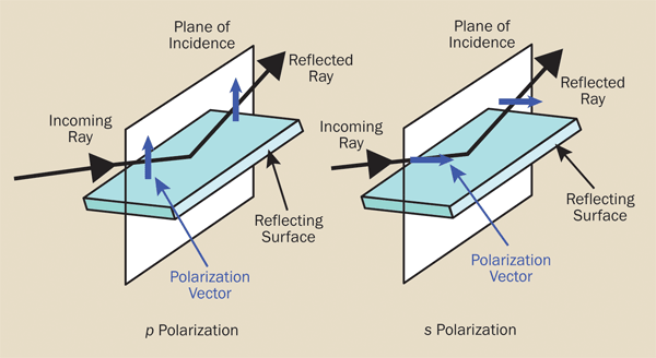
Figure 3. The electric field vector for p polarized light lies in the plane of incidence, while for s polarized light, it is perpendicular to the plane of incidence.
The reflectance of a dielectric interface is higher for s polarization than for p polarization at all nonzero angles of incidence. Therefore, if low reflectivity from a tilted component is desired, it is advantageous to design the geometry of the optical system so that the optic encounters p polarized light.
It is also important to note the distinction between unpolarized and randomly polarized light. Unpolarized light can be thought of as consisting of equal amounts of s and p polarized components. Random polarization means an unspecified polarized state, the direction or ellipticity of which are either unknown or changing with time. This represents something of a worst-case scenario, since it forces the coating designer to assume that specified performance must be met even under the least favorable circumstances. Ambient, incoherent light is unpolarized, for example, while laser light emerging from a single-mode fiber optic is typically randomly polarized.
The response of dielectric coatings shifts to shorter wavelengths as angle of incidence increases. In other words, an AR coating designed to produce minimum reflectance at normal incidence at 532 nm will instead deliver minimum reflectance at a shorter wavelength when used at 45° incidence. This can become a consideration when applying AR coatings on highly curved substrates. For example, on a steep aspheric lens, the angle of incidence at the center is 0°, while at the edge of the component, it might be 70°. This means that, even when working with a single wavelength, the coating must have broad bandwidth so that it still performs well at the nominal wavelength even when its response is shifted. Furthermore, actually applying films on such steep surfaces may require special tooling to maintain uniformity. Thus, the specifier of coatings for use under such conditions should be aware that there may be a significant trade-off in terms of the complexity and cost of that film versus the reflectance.
Antireflection coatings that work at two or more discrete wavelengths are common in laser applications. In general, it’s easier (and therefore more economical) to achieve high performance at a few individual wavelengths than it is to cover an entire band with the same performance level. Furthermore, specifying high performance at only one of the wavelengths and relaxing specifications at the other(s) will also generally keep the cost down.
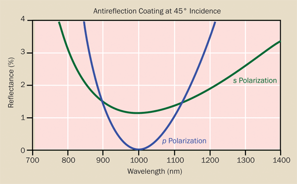
Figure 4. When used at higher angles of incidence, a significant difference exists in the reflectance of an antireflection coating between s and p polarizations.
Producing multiwavelength AR coatings that operate in both the ultraviolet and the visible, or in the visible and the infrared, can also be challenging because of the limited number of materials that simultaneously transmit in these regions. Specifically, only a limited number of coating materials can be used below 250 nm, so going shorter than this wavelength constrains design and drives up cost. On the other end of the spectrum, many materials that transmit in the visible don’t work above/about 5 µm. Thus, an AR coating that operates at both deep-UV and visible wavelengths is a challenge to produce, as is a coating intended for operation in the NIR range and at 10 µm.
Laser damage threshold is an important consideration in many applications. Designing a coating to maximize damage threshold may limit the choice of coating materials, designs, and processes, which in turn may make it more difficult to achieve a given performance target, such as absolute reflectance at a single wavelength or coating bandwidth.
High reflectors
For mirror coatings, probably the most important choice facing the consumer is whether to use a metal or metal-dielectric hybrid coating, versus an all-dielectric design. The primary advantage of metal coatings is very broad spectral bandwidth. For example, aluminum — the most commonly used mirror coating — has a reflectance of over 85% from 400 nm to well past 10 µm. Gold delivers over 99% reflectance from 2 µm well into the far-infrared. These levels of performance would be virtually impossible to achieve with all-dielectric coatings. In addition, the difference in reflectance between the s and p polarizations is usually substantially smaller for metal coatings than for all-dielectrics.
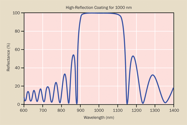
Figure 5. Reflectance of a typical narrowband high-reflection coating, in this case centered at 1000 nm.
However, the peak reflectance of metal films does not equal that which can be obtained with dielectric coatings. Even gold, which offers 99.5% reflectance in the infrared, cannot compare with dielectric coatings that can routinely deliver 99.99% reflectance or higher, albeit at a single wavelength. The small amount of absorption in metal films that limits their reflectance also contributes to another significant limitation: damage when exposed to high laser fluences.
Metal films are also less physically durable than all-dielectric coatings. Specifically, they have less resistance to abrasion, humidity, thermal cycling, and salt exposure than dielectrics. Silver in particular must always be covered with another material to prevent oxidization, which significantly lowers its reflectance.
For all-dielectric high reflectors, substrate quality is a consideration when specifying extremely high (≥99.995%) reflectivity because surface scatter becomes a performance-limiting factor. Thus, the surface roughness of the underlying substrate must be specified, and the consumer should expect that specifying a very smooth surface will drive up cost because it necessitates the use of specialized polishing techniques.
As with AR coatings, there is a trade-off in high reflectors between bandwidth and peak performance, although the effect is not as pronounced. Moreover, HR coatings typically contain numerous layers, so demanding very broadband performance can result in coatings that have increased scatter and absorption, as well as significant internal stress; the latter can require special measures to maintain a high level of surface figure accuracy.
Beamsplitters and partial reflectors
Nonpolarizing beamsplitters come in two basic forms: namely, cube and plate. Cube beamsplitters typically consist of two right-angle prisms mated at their hypotenuses. The beamsplitter coating is applied at this interface, while the input and output faces typically receive antireflection coatings. They are designed for normal incidence (on the input/output faces), and the reflected beam is displaced 90° from the input. Plate beamsplitters are typically constructed on a plano substrate: the beamsplitter coating is on the first side, and the second side may have an AR coating. These usually operate at 45° incidence and, again, the reflected beam is displaced 90° from the input. Another common type of partial reflector is a laser output coupler. These are generally on a curved substrate with a relatively long radius and work at normal incidence.
One feature of cube beamsplitters is that their performance tends to be less sensitive to input polarization than plate designs. The other major advantage of cube beamsplitters is that secondary reflections from the input and output faces overlap the main beam, whereas in plate beamsplitters they are offset.
One drawback of cube beamsplitters is that they are bulkier and heavier than plates, which can be a concern especially for larger aperture sizes. The other problem is that in most cube beamsplitters, the prisms are attached with adhesive or by optical contact. In either case, this can compromise performance by introducing wavefront errors. Furthermore, absorption in the adhesive can cause scatter and significantly reduce laser damage threshold.
Some leading manufacturers have developed methods for preparing the prism surfaces so that an actual chemical bond is formed when the components are assembled. Tests at REO show that this yields a component that has the same mechanical strength and ruggedness as a monolithic cube, yet which avoids the absorption, scatter and damage limitations of adhesive bonding.
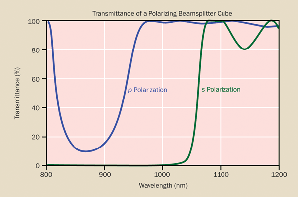
Figure 6. Polarizing coatings maximize the difference in reflectance between s and p polarizations to achieve high extinction ratios.
Several factors can drive complexity, and hence cost, in beamsplitters. For example, as angle of incidence increases, the growing difference in reflectivity for s and p polarizations makes it progressively more difficult to deliver a partial reflector that performs equally well for both polarization states. Thus, it’s advantageous to work with just a single polarization under these circumstances, if possible. However, if working with unpolarized light is inevitable, then it’s better to design an optical system in which beamsplitters operate at lower angles of incidence so as to minimize the effects of this split.
It’s also important to be careful regarding how tolerances are specified. There is a big difference between a beamsplitter that must maintain its nominal performance over the entire range of 45° ±5° incidence, versus one that must achieve nominal performance somewhere over that range. In the first case, the performance specification must be met at all angles over the 40° to 50° incidence range. In the second case, the performance specification is only met somewhere in the 40° to 50° incidence range, and it is expected that the user will place the component in his system and tilt-tune it to achieve the desired performance level. The first case demands a much more costly component than the second.
Bandwidth is again a big factor in beamsplitters. Making a polarization-insensitive coating that extends more than ±10% of the center wavelength (e.g., 550 nm ±50 nm) is a substantial challenge.
Polarizers
Thin-film polarizers also come in both cube and plate form, and many plate polarizers are designed for use at or near Brewster’s angle rather than 45° incidence. Brewster’s angle, which is the angle at which the p polarization reflectance drops to zero, is around 56° for visible wavelengths and glass substrates. Cube polarizers are typically designed for use at around 45°, although there can be performance benefits to higher angles of incidence. Many of the trade-offs associated with nonpolarizing beamsplitter cubes apply to cube polarizers as well; namely, cube construction is bulkier than plate construction, and the use of adhesive can limit laser damage resistance and compromise wavefront performance. Also, all the considerations mentioned earlier for nonpolarizing beamsplitters about specifying angular range and tilt-tuning still apply.
Typically, the most important performance specification for a polarizing beamsplitter is the extinction ratio — the ability to separate s and p polarizations. Polarizers are virtually always configured to pass p polarization and reflect s polarization. As a result, the transmission extinction ratio is defined to be the p transmission divided by the s transmission (Tp/Ts). Similarly, the reflection extinction ratio is defined to be the s reflection divided by the p reflection (Rs/Rp).
When specifying a system using polarizers, it is important to understand that it is much easier to eliminate s polarized light from the transmitted beam than it is to keep p polarized light out of the reflected beam. Therefore, a transmission extinction ratio of 10,000:1 is achievable, while a reflection extinction ratio of greater than 100:1 is difficult. Tightening the reflection extinction ratio specification will rapidly drive up cost, so these performance characteristics should be kept in mind during system design.
It is also challenging to produce thin-film polarizers that work over a broad range of wavelengths or at multiple wavelengths, as this will add tight constraints to the substrate and coating materials and the angle of incidence.
Filters
Filter coatings have separate highly transmissive and highly reflective or absorptive wavelength regions. When the rejected wavelengths are not of interest, bulk absorptive materials (e.g., colored glass) may be incorporated into the component to improve out-of-band rejection.
Figure 7 shows three typical transmission curves for long-wave pass thin-film filters. As the sloped section of the curve becomes steeper, the wavelength difference between the highly reflected and transmitted sections necessarily decreases. However, note that as curve slope increases, there is successively more “ringing” in the response of the transmission band. The problem is that the exact shape and peak locations of these oscillations are difficult to control during fabrication. As a result, as the reflected and transmitted wavelengths get closer together, it becomes increasingly difficult (and therefore expensive) to deliver high transmission at a specific wavelength. Where a transmission curve with a very sharp edge is critical (e.g., in Raman spectroscopy), designers sometimes use a holographic optical element instead of a dielectric filter.
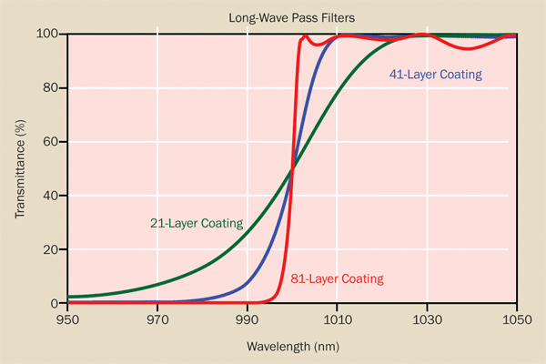
Figure 7. As layer count is increased in a long-wave pass filter design, the separation between the high and low transmission bands decreases, but at the expense of passband transmission.
The same process considerations also make it difficult to precisely control the wavelength at which the coating response transitions from reflection to transmission, and also limits the ability to control center wavelength in very narrow bandpass filters. Keeping this center wavelength tolerance relatively loose, and making up for it by allowing the optic to be tilt-tuned when actually used, can lower component cost.
Linear variable filters have spectral characteristics that shift as a function of position. They can be produced as bandpass filters, long pass filters, or short pass filters. Figure 8 provides an illustration of the spectral performance of a linear variable bandpass filter at different positions along its length. Critical aspects for these types of filters include out-of-band blocking, accuracy and linearity of the filter's slope, and the range of slopes that can be produced, which determines the range of possible sizes.
Figure 8a. Scan of a representative linear variable bandpass filter design illustrating the change in the transmission spectrum as a function of position along the filter's 10 mm length.
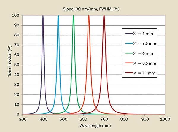
Figure 8b. A linear variable filter spectra calculated at five specific positions located along a 10 mm length.
High energy laser (HEL) reflective and transmissive coatings
Conditions required for survivable HEL coatings are unique and necessitate capabilities that ensure meeting critical requirements for coating absorption and defect levels. To be useful for HEL applications, optical components need to be of higher quality than standard optics, and the thin-film coatings require careful selection of materials and process technologies. Coatings should be applied with ultrapure materials, high-energy deposition processes (such as ion beam sputtering), and automated process control with OH management. Specialized metrology is needed to ensure process consistency and material conformance. Suppliers should have the capability to make applicable measurements using state-of-the-art techniques such as photothermal CPI with sensitivity < 0.2 ppm and laser measurements at 1064 nm, 940 nm, 532 nm, and 355 nm.
It has been reported that high energy laser components benefit from process optimization which leverage automated nondestructive surface metrology with large scale defect measurements to optimize laser damage survivability.
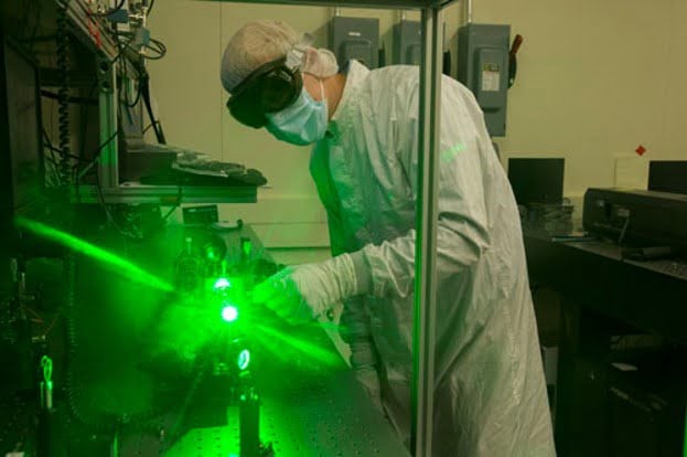
Metrology technician making a high sensitivity photothermal CPI absorption measurement to ensure optical coating process consistency and material conformance.
Coating fabrication
Thin-film coatings can be produced by several different technologies. Unfortunately, some manufacturers utilize only one or perhaps two methods and, understandably, they tend to emphasize the benefits of their favored technique(s). Over time, this has led to customer confusion and various misconceptions about the applicability and benefits of certain processes. In reality, there are multiple coating methods because they all have value: Each has unique advantages and limitations. One technique might be optimum for a demanding, multispectral laser application, while another might be best for producing a coating for a humid environment. Customers need not be experts in thin-film coating methods; however, it’s advantageous to know the features of the available methods. Also, working with a vendor who employs all or most of these techniques will likely bring better objectivity to the recommended solution.
E-beam and thermal evaporation
Evaporative coatings are produced in a high-vacuum chamber. Both metals and dielectric coating materials can be utilized with this technique. The coating material is heated either resistively or through electron beam bombardment until it vaporizes. The vapor then streams away from the source and recondenses on all surfaces that are in a line of sight with the source.
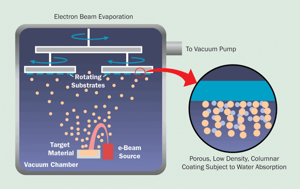
Figure 9. An electron beam vaporizes a target material, which deposits on the optical substrates.
Because no energy is applied as the vapor condenses and settles on the surface, thin films formed with this method are porous, of relatively low density and columnar in structure. Substrates are typically heated to several hundred degrees Celsius during the coating process to reduce this effect; however, it is by no means eliminated.
Porosity allows evaporative films to subsequently absorb moisture, meaning that the performance of the coating can shift in use with changes in ambient temperature and humidity. The low density also compromises mechanical durability to a certain extent, although these films can typically meet most of the MIL-SPEC durability and environmental requirements. Furthermore, the requirement to heat the components during processing can limit substrate material choice and also introduce stress in the substrate due to thermal cycling.
Evaporative coating processes are difficult to automate entirely and typically need monitoring by an operator. However, the high deposition rates keep coating run times relatively short and thus production costs low. As a result, this method is particularly favored when cost is a significant consideration and performance and durability specifications are relatively loose. The other big advantage of evaporative methods is that they are suitable for use with an extremely wide range of coating materials, from fluorides used in the deep-UV, to oxides for visible wavelengths, through semiconductor and sulfide materials often employed in the infrared.
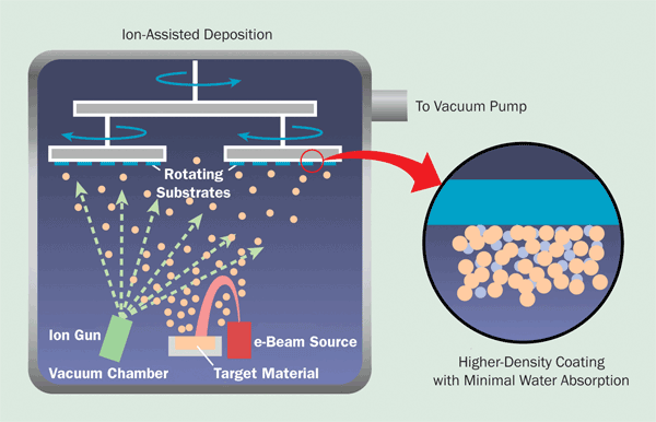
Figure 10. Adding an ion assist to electron beam evaporation produces a higher-density coating.
Ion-assisted deposition (IAD)
IAD utilizes the evaporative method described previously but adds a high-energy ion beam that is directed at the part to be coated. These ions impart energy to the deposited material — acting almost like an atomic-sized hammer — resulting in a higher film density than achieved with purely evaporative methods. The ion beam can also be used to preclean or etch the surface of the substrate, which can improve film adhesion. The combination of a relatively cold deposition process and the ion preclean affords the opportunity to coat plastic substrates such as polycarbonate lenses or visors, and even enables deposition on the ends of jacketed fibers and on the top of photoresist masks.
The higher density of IAD coatings generally gives them more mechanical durability, greater environmental stability, and lower scatter than evaporative films. Furthermore, the amount of energetic assistance can be varied from zero to a maximum level on a layer-by-layer basis, giving the process tremendous flexibility. For example, while IAD is not compatible with some of the commonly used materials in the infrared and deep-UV, it can be used solely on the outermost layer to yield an overall coating with superior durability. The ion energy can also modify the intrinsic stress of a film during deposition. In some cases, this can change the film stress from tensile to compressive. This can help to maintain substrate surface figure, especially when depositing thick infrared coatings.
Ion-beam sputtering (IBS)
In IBS, a high-energy ion beam is directed at a target typically composed of a metal or oxide. The ions transfer their momentum to the target material, causing atoms or molecules to sputter off. These high-energy atoms then deposit onto the parts to be coated. Oxygen is typically present in the coating chamber as a reactant to either create oxides when using metal targets, or to reoxidize any free atoms dissociated by the sputtering process when using oxide targets.
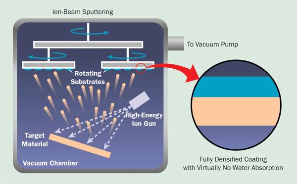
Figure 11. Ion-beam sputtering releases highly energetic particles from the target, resulting in the highest-density coatings attainable.
IBS produces uniform, completely amorphous films with high density (no porosity) and very strong adhesion. In addition, coated layers exhibit good adhesion and extremely low absorption and surface roughness (even into the subangstrom level). For example, in the visible and infrared, IBS films can have a combined scatter and absorption of less than 1 ppm.
While deposition rates are low compared with other coating techniques, control and reproducibility are high, making it possible to hit performance targets with greater precision than evaporative techniques. This makes IBS particularly well suited for producing steep edge filters, very broadband mirrors, and multiwavelength mirrors and AR coatings. In addition, the process can also be highly automated, meaning that it does not require operator supervision.
The biggest drawback of IBS is that it works only with a limited range of materials, typically metal oxides. Most of these aren’t transmissive below 250 nm or above/about 5 µm, although with carefully selected materials and process parameters, IBS films can be produced with high performance characteristics at wavelengths as short as 190 nm.
Magnetron sputtering
In magnetron sputtering, the target material is held at a negative voltage and immersed in a magnetic field. A plasma is created above the target, and ions are accelerated toward the material due to its negative potential. Ion collisions with the target cause material to be sputtered off. Secondary electrons are also emitted from the target; these are trapped by the magnetic field and serve to maintain the plasma through ionizing collisions.
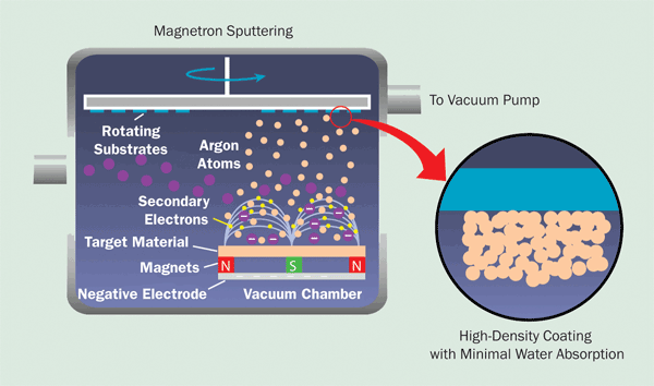
Figure 12. Magnetron sputtering releases target particles with lower energy than IBS, resulting in lower coating densities, but deposition rates are higher than with IBS, which reduces cost.
There are a number of variations on how magnetron sputtering is implemented, depending upon the desired target materials and deposition parameters. For example, pure metal targets can be biased with a DC power supply, while semiconductors and dielectrics typically require either radio frequency or pulsed DC. Deposition can take place with or without a reactive gas present, depending on whether the formation of oxides is desired.
Magnetron sputtering generally represents a midground between evaporative techniques and IBS in terms of cost, quality and performance. Specifically, it allows higher deposition rates than IBS and has access to essentially the same material set. The energy of the deposited atoms isn’t as high with magnetron sputtering as is achieved with IBS, but it is still superior to evaporative methods. Thus, coating durability and stability are excellent. One drawback of magnetron sputtering is that the source must generally be much closer to the part substrates than in other coating processes, which compromises both the coating uniformity (especially for parts with a steep radius of curvature) and surface quality as compared with IBS. It’s also difficult to control deposition parameters as closely with magnetron sputtering as can be accomplished with IBS, so the technique again lies in the middle in terms of the precision it can achieve. All this makes magnetron sputtering a good choice when film durability and stability, as well as cost, are important, but the ultimate performance in terms of precision, scatter and absorption is not required.
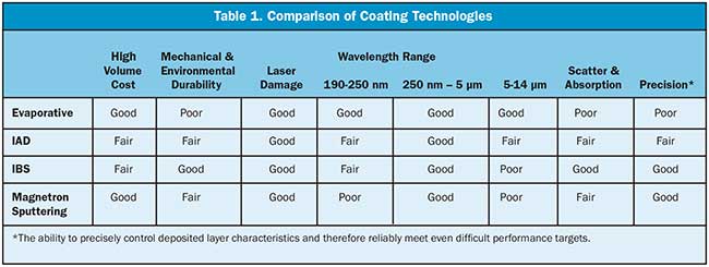
Table 1 provides a quick overview comparison of the different coating technologies. However, there are many different implementations of each of the techniques, so this information should serve only as the starting point in discussions with your coating supplier.
Conclusion
In conclusion, virtually all optical systems today utilize thin films in some way, and in many cases, system operation is critically dependent upon coating performance. Real-world coatings always involve trade-offs amongst various performance parameters and cost, and often a small change in specifications can have a significant impact. In addition, there are differences in the capabilities and cost characteristics of the various deposition technologies. Because of these factors, it’s often advantageous to partner with an optics and coatings vendor who offers a full gamut of design and fabrication capabilities, and who can select the optimum solution to meet all the critical constraints for a specific application.