A new thin-film deposition process based on magnetron sputtering is proving to be a cost-effective technique for fabricating high-precision filters for fluorescence techniques.
Dr. Georg J. Ockenfuss and Dr. Robert B. Sargent, JDSU Corp.
Fluorescence techniques are important in biological applications because they enable discrimination between different types of materials and structures. Instruments based on fluorescence techniques include flow cytometers, microarray scanners and various types of imaging systems, including fluorescence microscopes. Optical interference filters are key components for implementing fluorescence techniques because of their excellent filtering performance and competitive cost.
One popular and representative technique is fluorescence microscopy. A key element of a fluorescence microscope is the filter cube (Figure 1). Filters are employed in microscopy to isolate the excitation and emission bands of one or more fluorophores. The excitation filter transmits light that excites the fluorophore while rejecting or blocking other light. Light from the sample is processed by the emission filter, which transmits light emitted by the fluorophore while blocking all other light. It is especially important that the emission filter reject the excitation light that is scattered back from the sample, which may be very intense. A dichroic beamsplitter is used to maximize the signal-to-noise ratio by directing the appropriate excitation/emission light to the correct location.
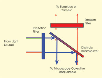
Figure 1. A filter cube is a key element in fluorescence microscopy because it contains filters to isolate the excitation and emission bands of one or more fluorophores.
Optimum excitation and emission filters are characterized by high transmission in their passbands (as close to unity as possible) and good blocking in other relevant spectral regions. The blocking level often is characterized by the optical density, which is the negative of the logarithm of the fractional transmission level. Hence unity (100%) transmission is equivalent to an optical density of 0, whereas one part per million transmission is equivalent to an optical density of 6.
The development of interference coating technology began in the 1930s, when improvements in vacuum pump technology enabled the formation of materials by evaporation in vacuum.1 By the 1960s, thin-film interference-based bandpass filters were readily available. These filters typically were made using alternating layers of zinc sulfide and cryolite, which were easy to deposit using thermal evaporation. Typical processes deposited filters at high rates using optical transmission monitoring to control the layer thicknesses, and these techniques still are employed today.
Improving performance
Films deposited using these so-called “soft coatings” are not very durable and must be sealed to protect them from any moisture penetration. This requires that the filters employ two or more glass substrates that seal the soft coatings within. This leads to a second disadvantage that occurs when images from two or more fluorophores are to be combined in a single image: The wedge introduced by the combination of these multiple sealed substrates can result in poor registration between the multiple images. Solutions that use a single glass substrate — and therefore require durable coatings — have the advantage that any such wedge may be eliminated through proper fabrication of the substrate. A measure of quality in this respect is how much shift is introduced by the wedge at the microscope image. If the shift is less than one pixel on the imaging detector, the filters are considered satisfactory and are sometimes referred to as having “zero pixel shift.”
Several approaches have been taken over the years to improve the performance and durability of interference filters. One has been continued evolution of the sealing technologies for soft coatings, while another has been the development of more robust coatings that are insensitive to the environment and that do not require sealing. For the near-ultraviolet, visible and near-infrared parts of the spectrum, metal oxides were recognized as having superior properties in this respect.
Today, energetic deposition processes such as ion-assisted deposition, ion beam sputtering and magnetron sputtering are widely employed in the production of optical interference coatings. All of these processes can deposit dense and robust coatings that do not require lamination or sealing.
Ion-assisted deposition employs an ion source in conjunction with an evaporation source. Ions from the source bombard the growing film, densifying it as it grows. Provided that sufficient bombardment occurs, dense coatings with a void-free microstructure are formed. Ion-assisted deposition was the first of the energetic deposition technologies to be deployed widely because it produces good-quality films at high deposition rates. However, the process does have limitations when used to deposit the most precise filters because of variability in the evaporation process.
Sputtering ahead
Ion beam sputtering uses an ion source to directly bombard a target with high-energy ions; ejected or “sputtered” material is deposited onto a part that becomes the filter. The technique was developed about the same time as ion-assisted deposition and initially was used in demanding applications such as laser ring gyro mirrors, which require extremely low loss and very low roughness. One disadvantage of the process is that its deposition rate is much slower than that of ion-assisted deposition, and for many applications it is not an economical process. Thus ion beam sputtering often is reserved for cases where the premium cost of the process is supported by the specialized application.
Magnetron sputtering uses a magnetic field to confine a plasma above a target. The target is held at a negative voltage so that ions from the plasma bombard it, and material ejected from the target is deposited on the part. Magnetron sputtering is an efficient and widely used process for depositing coatings and, when operated in a suitable low-pressure environment, produces high-quality dense coatings. The process produces films of quality similar to that of ion beam sputtering in most respects but with much higher deposition rates and correspondingly lower costs.
JDSU’s Ucp-1 filter coating process is a load-locked high-rate deposition process. At its heart is magnetron sputtering, which was selected because of its well-known ability to produce robust hard-oxide films, its inherent process stability and high deposition rate. Smaller deposition systems tend to be more precise, so the system was designed around a modest batch size of six 200-mm-diameter parts, similar to or somewhat larger than the size of other precision coating platforms such as those used for soft-coating technology and ion beam sputtering. The system was optimized to enable the magnetron-sputter deposition of metal oxide materials such as silicon dioxide at a high deposition rate of approximately 1nm/s.
Recently, the coating process has been applied to the fabrication of fluorescence filters. This application presents a serious challenge because many layers are required to achieve the steep edges and high blocking necessary. Accurate control of each layer is vital, as small errors lead to unacceptable deviations in filter performance. Finally, the thin-film materials must have low absorption and scatter to provide high transmission in the filter passbands.
Single-band filter sets
A common fluorophore used in fluorescence microscopy is GFP. In a filter set for GFP fabricated with Ucp-1, the transmission bands of the excitation and emission filters are very close to one another, and the transition slopes are extremely steep in the region between the passbands (Figure 2). These transition slopes cross one another at a wavelength of about 494 nm with a very high blocking value (optical density 6), which ensures excellent isolation between the excitation and emission bands. The excitation and emission filters both have an average passband transmission above 95 percent with a minimum transmission above 90 percent.
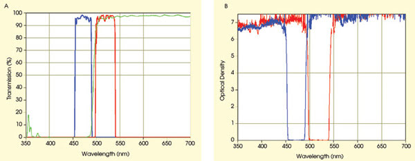
Figure 2. Measurements from a filter set for GFP show the excitation filter as blue, the emission filter as red and the dichroic beamsplitter as green. Measurements taken at a 0° angle of incidence for the excitation and emission filters and at a 45° angle of incidence for the beamsplitter are shown on a linear transmission scale (A) and on a logarithmic optical density scale (B).
A combination of high passband transmission and deep blocking at the fluorescence wavelengths of interest is fundamental, but it is not sufficient to ensure a high signal-to-noise ratio. Light beyond the fluorescence region contributes only to noise and must be blocked. The precise levels of blocking required depend on the system design and especially on the light source and detector type used. The example filters in Figure 2 incorporate out-of-band blocking exceeding optical density of 6 between 300 and 800 nm, and exceeding optical density of 5 between 800 and 1100 nm. These levels may be tailored readily to the instrument application at hand.
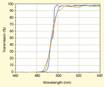
Figure 3. A theoretical plot of a beamsplitter for collimated light is shown as blue and for f/8 is shown as red. The actual measurement is green.
A beamsplitter is used at a 45° angle of incidence, and its performance is sensitive to the range of angles, or the f number, of the incident light. Instruments such as fluorescence microscopes typically use a low range of angles — or equivalently a high f number — thus, the light is nearly collimated. Spectrophotometers that characterize filters often use a light cone translating to an f number of about 8. Figure 3 compares the theoretical performance of a GFP beamsplitter calculated for collimated light, the calculated performance of the GFP beamsplitter in an f/8 beam and the measured performance of a Ucp-1 deposited GFP beamsplitter. The measurements were obtained using a Cary 5000 spectrophotometer with an f/8 beam from Varian Inc. of Palo Alto, Calif. Note that the f/8 calculation and measured performance agree well and that the slope of the filter used with f/8 light is clearly less steep than with collimated light.
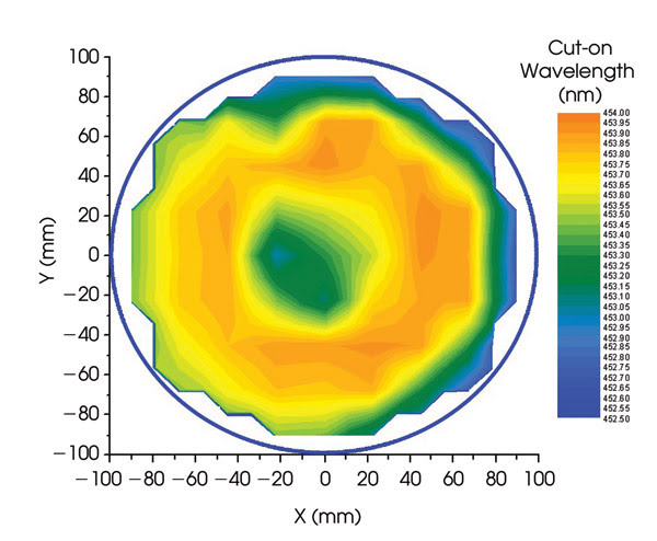
Figure 4. The Ucp-1 process produces uniform filters as seen in this contour plot of the 50 percent cut-on wavelength for a GFP excitation filter across a 200-mm-diameter wafer. The blue circle indicates the edge of the wafer.
The Ucp-1 platform produces filters with excellent uniformity. Figure 4 shows a spectral placement map of the GFP excitation filter coated on a 200-mm fused-silica wafer. The spectral placement was calculated from the relative 50 percent points at the cut-on edge (near 453 nm) of the excitation filter shown in Figure 2. The maximum and minimum values on the wafer are only 0.28 percent apart. The ability to deposit precision filters on large areas is important in a few applications, and this demonstration illustrates how high-precision filters can be produced at modest cost in moderate volume.
The highly precise layer thickness control of the platform enables the fabrication of very complicated filter designs, such as a triple-bandpass set for simultaneous detection of three fluorophores (Figure 5). These filters have passband peak transmissions greater than 90 percent and very good isolation exceeding an optical density of 5 between the passbands.
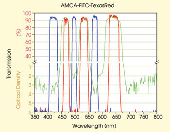
Figure 5. The measured results for a filter set for the fluorophores AMCA, FITC and TexasRed are shown. The excitation filter measurements are blue, emission filter red and dichroic beamsplitter green.
Filters made using energetic deposition processes are displacing soft-coated filters in many biomedical applications, including fluorescence microscopy, because of their durability, excellent spectral filtering ability and the ease of providing “zero pixel shift” for those applications that require it. In the past, the premium performance of energetic deposition processes such as ion beam sputtering have been saddled with the high cost of these inefficient processes, but new technology provides a new optical filter alternative to OEM manufacturers of optical instruments — single-substrate, zero-pixel-shift filters with excellent spectral performance at reasonable cost.
Meet the authors
Georg J. Ockenfuss is senior development engineer and Robert B. Sargent is coating development manager for JDSU’s Custom Optics Product Group in Santa Rosa, Calif.
References
1. H.A. Macleod (2001). Thin-Film Optical Filters, 3rd edition, Institute of Physics Publishing, London.